HP BL680c Memory technology evolution: an overview of system memory technologi
HP BL680c - ProLiant - G5 Manual
 |
UPC - 884420396314
View all HP BL680c manuals
Add to My Manuals
Save this manual to your list of manuals |
HP BL680c manual content summary:
- HP BL680c | Memory technology evolution: an overview of system memory technologi - Page 1
...11 Double Data Rate SDRAM technologies 11 DDR-1 ...11 DDR-2 ...13 DDR-3 ...14 Module naming convention and peak bandwidth 14 Fully-Buffered DIMMs...15 FB-DIMM architecture...16 Challenges ...17 Rambus DRAM ...18 Importance of using HP-certified memory modules in ProLiant servers 19 Conclusion - HP BL680c | Memory technology evolution: an overview of system memory technologi - Page 2
applications are driving the need for better memory technologies for servers and workstations. Consequently, there are several memory technologies on the market at any given time. HP evaluates developing memory technologies in terms of price, performance, and backward compatibility and implements - HP BL680c | Memory technology evolution: an overview of system memory technologi - Page 3
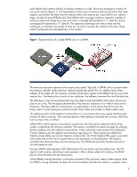
The command portion of the address/command bus conveys instructions such as read, write, or refresh. When FPM or EDO memory writes data to a particular cell, the location where the data will be written is selected by the memory controller. The memory controller first selects the page by strobing the - HP BL680c | Memory technology evolution: an overview of system memory technologi - Page 4
Representation of a write operation for FPM or EDO RAM DRAM storage density and power consumption The storage capacity (density) of DRAM is converted to number of memory bus clocks. Chipsets and system bus timing All computer components that execute instructions or transfer data are controlled by - HP BL680c | Memory technology evolution: an overview of system memory technologi - Page 5
components in a typical server are controlled by data or instructions due to clock resynchronization. In contrast, synchronized components know on which clock cycle data will be available, thus eliminating these timing delays. Memory memory subsystem are the memory timing and the maximum DRAM speed - HP BL680c | Memory technology evolution: an overview of system memory technologi - Page 6
after the first access (6-1-1-1) before the memory controller has to send another CAS. Figure 4. Burst mode access. NOP is a "No Operation" instruction. Clock Command Address Data Active NOP NOP Read NOP NOP NOP NOP NOP NOP Row Col Data Data Data Data 64b 64b 64b 64b SDRAM technology FPM - HP BL680c | Memory technology evolution: an overview of system memory technologi - Page 7
Bank interleaving SDRAM divides memory into two to four banks for simultaneous access to more data. This division and simultaneous access is known as interleaving. Using a notebook analogy, two-way interleaving is like dividing each page in a notebook into two parts and having two assistants to each - HP BL680c | Memory technology evolution: an overview of system memory technologi - Page 8
or all of the DRAM chips on a DIMM. For an ECC DIMM, a memory rank is a block of 72 data bits (64 bits plus 8 ECC bits). A single-rank ECC DIMM (x4 or are staggered so that both sets of DRAM chips do not contend for the memory bus at the same time. Quad-rank DIMMs with ECC produces four 72-bit - HP BL680c | Memory technology evolution: an overview of system memory technologi - Page 9
number of DIMM slots on a bus at higher speeds, modern chipsets employ multiple memory buses. If the total number of ranks in the populated DIMM slots exceeds the maximum number of loads the chipset can support, the server may not boot properly or it may not operate reliably. Some systems check the - HP BL680c | Memory technology evolution: an overview of system memory technologi - Page 10
called channel interleaving. In channel interleaving, each integrated memory controller successively provides a 64-byte cache line of data from the first DIMM on its channel. After the last memory controller completes the data transfer, the memory controllers can provide a cache line from a second - HP BL680c | Memory technology evolution: an overview of system memory technologi - Page 11
3.2 GB/s, which is 400 percent more than original SDRAM. Prefetching In SDRAM, one bit per clock cycle is transferred from the memory cell array to the input/output (I/O) buffer or data queue (DQ). The I/O buffer releases one bit to the bus per pin and clock cycle (on the rising edge of the - HP BL680c | Memory technology evolution: an overview of system memory technologi - Page 12
. Instead of using a 3.3-V operating voltage, DDR-1 uses a 2.5-V signaling specification known as Stub Series-Terminated Logic_2 (SSTL_2). This low-voltage signaling results in lower power consumption and improved heat dissipation. Stobe-based data bus SSTL_2 signaling allows DDR-1 to run at faster - HP BL680c | Memory technology evolution: an overview of system memory technologi - Page 13
used in desktop PCs or servers. To vary the cost of DDR-1 DIMMs for these different markets, memory manufacturers provide unbuffered and registered same memory subsystem. DDR-2 DDR-2 SDRAM is the second generation of DDR SDRAM. It offers data rates of up to 6.4 GB/s, lower power consumption, - HP BL680c | Memory technology evolution: an overview of system memory technologi - Page 14
support "write leveling" on DDR-3 DIMMs. • 1.5-V signaling (compared to 1.8 V for DDR-2) for lower power consumption • A thermal sensor integrated on the DIMM module signals the chipset to throttle memory was based on the effective clock rate of the data transfer: PC200 for DDR SDRAM that operates at - HP BL680c | Memory technology evolution: an overview of system memory technologi - Page 15
rates ranging from PC 100 to DDR-3 1600. Note that the number of supported loads drops from eight to two as data rates increase to DDR2 800. Figure 14. Maximum number of loads per channel based on DRAM data rate. Increasing the number of channels to compensate for the drop in capacity per channel - HP BL680c | Memory technology evolution: an overview of system memory technologi - Page 16
specification, a serial interface that eliminates the parallel stub-bus topology and allows higher memory bandwidth while maintaining or increasing memory to the next FB-DIMM on the channel. Each AMB decodes the command data and ignores the commands that are targeted for a different DIMM. The - HP BL680c | Memory technology evolution: an overview of system memory technologi - Page 17
Challenges The challenges for the FB-DIMM architecture include latency and power use (thermal load). Memory latency is the delay from the time the data is requested to the time when the data is available from the memory controller. The FB-DIMM architecture increases this latency in two ways: - HP BL680c | Memory technology evolution: an overview of system memory technologi - Page 18
to support a maximum of 256 devices. However, using the repeater chips will add 1 to 1.5 clocks of additional delay. To account for differences in distance of the devices on the channel, more latency in increments of the clock can be added. This allows the memory controller to receive data from - HP BL680c | Memory technology evolution: an overview of system memory technologi - Page 19
and availability for ProLiant servers. The costs of system downtime, data loss, and reduced productivity caused by lower quality memory are far greater than the price difference between HP-certified memory and third-party DIMMs. Second, use of HP memory option kits prevents improper mixing - HP BL680c | Memory technology evolution: an overview of system memory technologi - Page 20
refer to the resources listed below. Resource description JEDEC Web site HP Advanced Memory Protection Fully-Buffered DIMM technology in HP ProLiant servers Web address http://www.jedec.org http://h18004.www1.hp.com/products/servers/technology/whitepapers/advtechnology.html#mem http://h18004.www1
-
 1
1 -
 2
2 -
 3
3 -
 4
4 -
 5
5 -
 6
6 -
 7
7 -
8
-
9
-
10
-
11
-
12
-
13
-
14
-
15
-
16
-
17
-
18
-
19
-
20
 |
 |

Memory technology evolution: an overview
of system memory technologies
technology brief, 8
th
edition
Abstract
..............................................................................................................................................
2
Introduction
.........................................................................................................................................
2
Basic DRAM operation
.........................................................................................................................
2
DRAM storage density and power consumption
...................................................................................
4
Memory access time
.........................................................................................................................
4
Chipsets and system bus timing
..........................................................................................................
4
Memory bus speed
...........................................................................................................................
5
Burst mode access
............................................................................................................................
5
SDRAM technology
..............................................................................................................................
6
Bank interleaving
.............................................................................................................................
7
Increased bandwidth
........................................................................................................................
7
Registered SDRAM modules
..............................................................................................................
7
DIMM Configurations
.......................................................................................................................
8
Single-sided and double-sided DIMMs
............................................................................................
8
Single-rank, dual-rank, and quad-rank DIMMs
.................................................................................
8
Rank interleaving
..........................................................................................................................
9
Memory channel interleaving
..........................................................................................................
10
Advanced memory technologies
..........................................................................................................
11
Double Data Rate SDRAM technologies
............................................................................................
11
DDR-1
.......................................................................................................................................
11
DDR-2
.......................................................................................................................................
13
DDR-3
.......................................................................................................................................
14
Module naming convention and peak bandwidth
...........................................................................
14
Fully-Buffered DIMMs
......................................................................................................................
15
FB-DIMM architecture
..................................................................................................................
16
Challenges
................................................................................................................................
17
Rambus DRAM
..............................................................................................................................
18
Importance of using HP-certified memory modules in ProLiant servers
.......................................................
19
Conclusion
........................................................................................................................................
19
For more information
..........................................................................................................................
20
Call to action
....................................................................................................................................
20