Hitachi 43FDX01B Service Manual
Hitachi 43FDX01B Manual
 |
View all Hitachi 43FDX01B manuals
Add to My Manuals
Save this manual to your list of manuals |
Hitachi 43FDX01B manual content summary:
- Hitachi 43FDX01B | Service Manual - Page 1
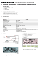
Television Module LGE PDP 2K6 PDP42X3* Contents Page 1. Technical Specifications, Connections, and Chassis Overview 2 2. Safety Instructions, Warnings, and Notes 5 3. Directions for Use 6 4. Mechanical Instructions 7 5. Service Modes, Error Codes, and Fault Finding 12 6. Block Diagrams - Hitachi 43FDX01B | Service Manual - Page 2
part and a Drive part. The Panel part consists of Electrodes, Phosphor, various dielectrics, and gas, while the Drive part includes electronic circuitry and PWBs. 1.1.1 General Specification Table 1-1 General Specifications Model 1 % white window, white window pattern at centre) Max. 330 W (Full - Hitachi 43FDX01B | Service Manual - Page 3
Technical Specifications, Connections, and Chassis Overview LGE PDP 2K6 1. EN 3 PCB PART NO. G_16390_008.eps 040806 Figure 1-4 Part number printing (on board) BOARD ASSY PART NR. BOARD NAME BOARD SERIAL NR. G_16390_005.eps 020806 Figure 1-5 Part number label (on board) TCP SERIAL NO. - Hitachi 43FDX01B | Service Manual - Page 4
EN 4 1. LGE PDP 2K6 1.1.3 Chassis Overview Technical Specifications, Connections, and Chassis Overview Y Driver Board Y Sus Board X Left Board PSU 3501Q00203B Control Board Figure 1-7 PWB location Z Sus Board X Right Board G_16391_002.eps 290607 - Hitachi 43FDX01B | Service Manual - Page 5
resistor or metal film resistor) in order to repair, insert it 10 mm away from a board. 15. During repairs, high voltage or high temperature components must be put away from a lead line. 16. This is a cold chassis but you better use an isolation transformer for safety during repairs. If repairing - Hitachi 43FDX01B | Service Manual - Page 6
EN 6 3. LGE PDP 2K6 3. Directions for Use Not applicable. Directions for Use - Hitachi 43FDX01B | Service Manual - Page 7
Mechanical Instructions 4. Mechanical Instructions Index of this chapter: 4.1 Mechanical Overviews 4.2 Panel/assy removal 4.2.1 Power Supply Unit 4.2.2 Control Board 4.2.3 Y Sustain Board 4.2.4 Y Driver Board 4.2.5 Z-Sustain board 4.2.6 X-board 4.1 Mechanical Overviews LGE PDP 2K6 4. EN 7 8 7 - Hitachi 43FDX01B | Service Manual - Page 8
EN 8 4. LGE PDP 2K6 Mechanical Instructions Figure 4-2 Label location on PWB's G_16390_014.eps 070806 Figure 4-3 Label indication G_16390_013.eps 070806 - Hitachi 43FDX01B | Service Manual - Page 9
3315Q-E037C and 3315Q-E037F . 5. Manufacture Serial No. Label of Module 2 1 1 2 G_16390_030.eps 220806 Figure 4-7 Control board removal 1 Model Name Model Names for Philips are PDP42X3A062, PDP42V7A012, PDP42V74112, PDP42V74102, PDP42V74012, PDP42V74002, PDP42V70102 and PDP42V70002. * PDP42V7 - Hitachi 43FDX01B | Service Manual - Page 10
EN 10 4. LGE PDP 2K6 Mechanical Instructions 4.2.3 Y Sustain Board 1. Unplug the connectors [1]. 2. Remove the fixation screws [2]. 3. Slide the board to the right, while unplugging connectors [3]. Do not touch the heatsink! 2 3 2 2 1 2 3 2 2 1 1 2 G_16390_031.eps 010906 Figure 4-8 Y-SUS - Hitachi 43FDX01B | Service Manual - Page 11
Instructions LGE PDP 2K6 4.2.5 Z-Sustain board 1. Unplug the connectors [1]. 2. Remove the fixation screws [2]. 3. Slide the board to the right, while unplugging connectors [3]. Do not touch the heatsink! 4. Pull out the locks of the FPC's [3} as indicated by the arrows. 5. Condition in Lock part - Hitachi 43FDX01B | Service Manual - Page 12
PDP 2K6 Service Modes, Error Codes, and Fault Finding 5. Service Modes, Error Trouble Shooting No display? N Vertical defect? N Horizontal defect? N Mis -discharge on screen? Check model No. of module, all connectors and cables. Y Partially no display? Y Check signal cables from Ctrl Board - Hitachi 43FDX01B | Service Manual - Page 13
Service Modes, Error Codes, and Fault Finding 5.1.1 No Display Check each section with following method. If there is a problem, replace or repair that part. If can cause a specific board to fail. LGE PDP 2K6 5. EN 13 G_16390_039.eps 110806 Figure 5-3 Control + Y-SUS board G_16390_042.eps 010906 - Hitachi 43FDX01B | Service Manual - Page 14
EN 14 5. LGE PDP 2K6 Service Modes, Error Codes, and Fault Finding PSU (see figure "PSU trouble shooting") 1. Check each unit part of PSU inside with naked eye (capacitor, FET, IC, resistor). 2. Check fuse. 3. Check output voltage, which is converted from AC to DC. 4. Voltage Check (5V, Va, Vs). - Hitachi 43FDX01B | Service Manual - Page 15
signal to the TCP. So, if there is a bar defect on screen, it may be a Control board problem. MCM Buffer IC Array Resistor 6 line R - array TCP 192 Line output F_15590_082.eps 060705 Figure 5-13 Control board address flow 5.1.3 Line Defect (Vertical) In case of one line open or shorted, check for - Hitachi 43FDX01B | Service Manual - Page 16
output pin. Normal diode value= 0.6 (forward) Normal diode value= OL (reverse) F_15590_087.eps 060705 Figure 5-18 Scan IC output diode check 5.1.5 Line Defect (Horizontal) FPC Check In case of one or more horizontal lines, this is probably due to FPC or panel inside the Control board. Y board - Hitachi 43FDX01B | Service Manual - Page 17
Service Modes, Error Codes, and Fault Finding Scan IC Check Check diode value of the right side part of the output pin. LGE PDP 2K6 5. EN 17 F_15590_091.eps 290605 Figure 5-20 Scan IC output diode check 5.1.6 Mis-discharge Defect Most of mis-discharge appearance is a problem of the Y-DRV, Y-SUS, - Hitachi 43FDX01B | Service Manual - Page 18
EN 18 5. LGE PDP 2K6 Service Modes, Error Codes, and Fault Finding Figure 5-23 Output waveforms on X, Y, and Z-boards G_16390_043.eps 300806 - Hitachi 43FDX01B | Service Manual - Page 19
unusual pattern of the Data TCP IC unit as shown in the picture below, check the fixation of the relevant X board. If that doesn't help, replace the X board. 2. In case of "Case 1": - Check the connection between the Data TCP connector and the IC. - Replace the relevant X board, or the Control board - Hitachi 43FDX01B | Service Manual - Page 20
the output wave with an oscilloscope (> 200 MHz) and compare the waveform with the waveform in the figure below. Adjust the Y board Set_up voltage (Vsetup) and time-interval "A" by changing VR3 and VR2. Check if -Vy and Vscan have been set correctly with VRy and VRsc respectively, to the value - Hitachi 43FDX01B | Service Manual - Page 21
wave. G_16390_049.eps 150806 Figure 5-35 IPM normal output FET assy (Y board: HS2) When the Set_up FET (2nd FFT of HS2) is damaged, there will be no picture. • Test Point: GND-Waveform (Y-DRV board) • Measuring condition: full white pattern. • Wave format: as shown in the figure below. G_16390_050 - Hitachi 43FDX01B | Service Manual - Page 22
22 5. LGE PDP 2K6 Service Modes, Error Codes, and Fault Finding - Test Point: Output TP of GND-TCP - Wave format: As shown in figure below. In case of normal wave output, when STB signal is generated, the output must maintain "HIGH". When STB signal is generated again, the output must fall to "LOW - Hitachi 43FDX01B | Service Manual - Page 23
Service Modes, Error Codes, and Fault Finding LGE PDP 2K6 5. EN 23 ZUZ} F_15590_036.eps 040705 Figure 5-43 Crystal normal output XU\}¥Y} vœ›—œ›G G–G›ŒGšŽ•ˆ“GšG“–ž p› ”ˆ GŠˆ•ŽŒG›ŒG SG F_15590_035.eps 060605 Figure 5-44 Crystal defective output - Hitachi 43FDX01B | Service Manual - Page 24
EN 24 5. LGE PDP 2K6 Service Modes, Error Codes, and Fault Finding 5.3 Defect Description Form spec. - Burn in (Plasma TV) / Sticking image (LCD TV) - MURA These symptoms are not claimable. Defect Board Spare Part Nr. 1. 2. 3. 4. Serial Nr. New Board Spare Part Nr. Serial Nr. BOARD REPAIR - Hitachi 43FDX01B | Service Manual - Page 25
Interface Controller Memory Controller Driver Timing Controller Display data, Driver timing (External Power) Vs (175V~190V) Va (60+ 1V) Vcc (5V) Scan Driver Common sustain driver Color PDP 1024 X 768 pixels Address Driver ත Applied Voltage level is specified at the time when Full-White pattern - Hitachi 43FDX01B | Service Manual - Page 26
turning "off". * Module "ON" : 5V => Va => Vs, Module "OFF": Vs => Va => 5V (4) Signal generator should be selected with 1024 x 768 (XGA) mode Adjustment 1. Measure the Vs voltage (180...195 VDC) on pin 10 of CN806 on the PSU board (see Figure "PSU Alignment"). The voltage should have the same value - Hitachi 43FDX01B | Service Manual - Page 27
to the value indicated on the voltage sticker with potentiometer VRy on the Y-SUS board. Y -SUS Set-up Voltage Waveform Adjustment Now connect the oscilloscope between the Waveform test point on the Y-Driver board and GND (see Figure ""Y-SUS Alignment"). Trigger with Vs-DA on the Control board (see - Hitachi 43FDX01B | Service Manual - Page 28
Alignment"). 2. Adjust Vzb to 100 ± 0.5 V with potentiometerVRzb on the Z-SUS board. 8.2.6 Internal Test Patterns The CTRL board is capable of generating its own video test patterns. To generate the test patterns, do as follows: • Disconnect the mains cord. • Disconnect the SSB of the TV set, by - Hitachi 43FDX01B | Service Manual - Page 29
9. EN 29 9. Circuit Descriptions, Abbreviation List, and IC Data Sheets Index of this chapter: 9.1 Introduction 9.2 Power Supply Unit (PSU) 9.3 Control Board 9.4 X Board 9.5 Y Sustain Board 9.6 Y Drive Board 9.7 Z Sustain Board 9.8 DC/DC Converter Part 9.9 FPC (Flexible Printed Circuit) 9.10 FFC - Hitachi 43FDX01B | Service Manual - Page 30
IC low, picture is changed to BLACK pattern. Signal is operated by synchronized vertical signal. ත The panel will not malfunction, if DISPEN is high at start up. G_16390_080.eps 310806 Figure 9-2 Power supply sequence 9.3 Control Board 9.3.1 Purpose Creates signal processing, and controls - Hitachi 43FDX01B | Service Manual - Page 31
Components IPM, diodes, electrolytic capacitors, and FETs. G_16390_025.eps 100806 9.6 Y Drive Board 9.6.1 Purpose • To supply Sustain, Reset waveform, made by the Y-SUS board, to the PDP through the SCAN DRIVER IC. • To supply a waveform that selects the horizontal electrodes (Y SUSTAIN electrodes - Hitachi 43FDX01B | Service Manual - Page 32
Descriptions, Abbreviation List, and IC Data Sheets 9.8 DC/DC Converter Part 9.9 FPC (Flexible Printed Circuit) 9.8.1 Purpose From 5V, Vs, and Va (from the PSU), the DC/DC converter makes 5V, 15V, Vy, Vsc, 5Vf, and Va, which are essential for each board. PSU YSUS Board 5V 5V 9.9.1 Purpose To - Hitachi 43FDX01B | Service Manual - Page 33
CLK COF CTRL DC FET FPC I/O IC IPM LED LGE MCM PCB PDP PFC PSU PWB RGB STB TCP Alternating Current Board Clock signal Chip On Flex / Foil / Film Control (board) Direct Current Field Effect Transistor Flexible Printed Circuit Input/Output Integrated Circuit Intelligent Power Module Light Emitting - Hitachi 43FDX01B | Service Manual - Page 34
text and graphics to PSU model 3501Q00201A (not used in this PDP model) changed to references to PSU model 3501Q00203B. • Corrections in texts referring to the PSU, Y-SUS and ZSUS boards. Manual xxxx xxx xxxx.2 • Text on how to generate Internal Test Patterns added to Chapter 8, Alignments. • Minor
-
 1
1 -
 2
2 -
 3
3 -
 4
4 -
 5
5 -
 6
6 -
 7
7 -
8
-
9
-
10
-
11
-
12
-
13
-
14
-
15
-
16
-
17
-
18
-
19
-
20
-
21
-
22
-
23
-
24
-
25
-
26
-
27
-
28
-
29
-
30
-
31
-
32
-
33
-
34
 |
 |

Published by MW 0765 BG CD Customer Service
Printed in the Netherlands
Subject to modification
EN
3122 785 16392
©
Copyright 2007 Philips Consumer Electronics B.V. Eindhoven, The Netherlands.
All rights reserved. No part of this publication may be reproduced, stored in a
retrieval system or transmitted, in any form or by any means, electronic,
mechanical, photocopying, or otherwise without the prior permission of Philips.
Colour Television
Module
LGE PDP 2K6
PDP42X3*
Contents
Page
1.
Technical Specifications, Connections, and Chassis
Overview
2
2.
Safety Instructions, Warnings, and Notes
5
3.
Directions for Use
6
4.
Mechanical Instructions
7
5.
Service Modes, Error Codes, and Fault Finding
12
6.
Block Diagrams, Test Point Overviews, and
Waveforms
25
7.
Circuit Diagrams and PWB Layouts
25
8.
Alignments
26
9.
Circuit Descriptions, Abbreviation List, and IC Data
Sheets
29
10. Spare Parts List
34
11. Revision List
34