Intel 925 Data Sheet - Page 113
PCICMD1-PCI Command D1:F0
 |
UPC - 683728067724
View all Intel 925 manuals
Add to My Manuals
Save this manual to your list of manuals |
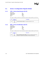
Page 113 highlights
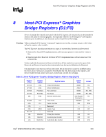
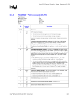
Host-PCI Express* Graphics Bridge Registers (D1:F0) R 8.1.3 PCICMD1-PCI Command (D1:F0) PCI Device: Address Offset: Default Value: Access: Size: 1 04h 0000h RO, R/W 16 bits Bit 15:11 10 9 8 7 6 5 4 3 Access & Default R/W 0b RO 0b R/W 0b R/WO 0b RO 0b RO 0b RO 0b Description Reserved INTA Assertion Disable: 0 = This device is permitted to generate INTA interrupt messages. 1 = This device is prevented from generating interrupt messages. Any INTA emulation interrupts already asserted must be de-asserted when this bit is set. Only affects interrupts generated by the device (PCI INTA from a PME or Hot Plug event) controlled by this command register. It does not affect upstream MSIs, upstream PCI INTA-INTD asserts and de-assert messages. Fast Back-to-Back Enable (FB2B): Not Applicable or Implemented. Hardwired to 0. SERR Message Enable (SERRE1): This bit is an enable bit for Device 1 SERR messaging. The MCH communicates the SERRB condition by sending an SERR message to the Intel® ICH6. This bit, when set, enables reporting of non-fatal and fatal errors to the Root Complex. Note that errors are reported if enabled either through this bit or through the PCI Express* specific bits in the Device Control Register 0 = The SERR message is generated by the MCH for Device 1 only under conditions enabled individually through the Device Control Register. 1 = The MCH is enabled to generate SERR messages which will be sent to the ICH6 for specific Device 1 error conditions that are individually enabled in the BCTRL1 register and for all non-fatal and fatal errors generated on the primary side of the virtual PCI to PCI Express bridge (not those received by the secondary side). The error status is reported in the PCISTS1 register. Reserved Parity Error Enable (PERRE): This bit controls whether or not the Master Data Parity Error bit in the PCI Status register can bet set. 0 = Master Data Parity Error bit in PCI Status register cannot be set. 1 = Master Data Parity Error bit in PCI Status register can be set. VGA Palette Snoop: Hardwired to 0. Memory Write and Invalidate Enable (MWIE): Hardwired to 0. Special Cycle Enable (SCE): Hardwired to 0. Intel® 82925X/82925XE MCH Datasheet 113
-
 1
1 -
2
-
3
-
4
-
5
-
6
-
7
-
8
-
9
-
10
-
11
-
12
-
13
-
14
-
15
-
16
-
17
-
18
-
19
-
20
-
21
-
22
-
23
-
24
-
25
-
26
-
27
-
28
-
29
-
30
-
31
-
32
-
33
-
34
-
35
-
36
-
37
-
38
-
39
-
40
-
41
-
42
-
43
-
44
-
45
-
46
-
47
-
48
-
49
-
50
-
51
-
52
-
53
-
54
-
55
-
56
-
57
-
58
-
59
-
60
-
61
-
62
-
63
-
64
-
65
-
66
-
67
-
68
-
69
-
70
-
71
-
72
-
73
-
74
-
75
-
76
-
77
-
78
-
79
-
80
-
81
-
82
-
83
-
84
-
85
-
86
-
87
-
88
-
89
-
90
-
91
-
92
-
93
-
94
-
95
-
96
-
97
-
98
-
99
-
100
-
101
-
102
-
103
-
104
-
105
-
106
-
107
-
 108
108 -
 109
109 -
 110
110 -
 111
111 -
 112
112 -
 113
113 -
 114
114 -
 115
115 -
 116
116 -
 117
117 -
 118
118 -
119
-
120
-
121
-
122
-
123
-
124
-
125
-
126
-
127
-
128
-
129
-
130
-
131
-
132
-
133
-
134
-
135
-
136
-
137
-
138
-
139
-
140
-
141
-
142
-
143
-
144
-
145
-
146
-
147
-
148
-
149
-
150
-
151
-
152
-
153
-
154
-
155
-
156
-
157
-
158
-
159
-
160
-
161
-
162
-
163
-
164
-
165
-
166
-
167
-
168
-
169
-
170
-
171
-
172
-
173
-
174
-
175
-
176
-
177
-
178
-
179
-
180
-
181
-
182
-
183
-
184
-
185
-
186
-
187
-
188
-
189
-
190
-
191
-
192
-
193
-
194
-
195
-
196
-
197
-
198
-
199
-
200
-
201
-
202
-
203
-
204
-
205
-
206
-
207
-
208
-
209
-
210
-
211
-
212
-
213
-
214
-
215
-
216
-
217
-
218
-
219
-
220
-
221
-
222
-
223
-
224
-
225
-
226
-
227
-
228
-
229
-
230
-
231
-
232
-
233
-
234
-
235
-
236
-
237
-
238
-
239
-
240
-
241
-
242
 |
 |