Intel 925 Data Sheet - Page 116
RID1-Revision Identification D1:F0, CC1-Class Code D1:F0 - 925x express chipset
 |
UPC - 683728067724
View all Intel 925 manuals
Add to My Manuals
Save this manual to your list of manuals |
Page 116 highlights
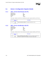
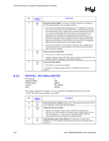
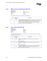
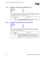
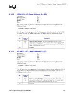
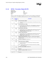
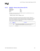
Host-PCI Express* Graphics Bridge Registers (D1:F0) R 8.1.5 RID1-Revision Identification (D1:F0) PCI Device: Address Offset: Default Value: Access: Size: 1 08h See table below RO 8 bits This register contains the revision number of the MCH device 1. Bit Access & Default Description 7:0 RO Revision Identification Number (RID1): This field indicates the number of times 00h that this device in this component has been "stepped" through the manufacturing process. It is always the same as the RID values in all other devices in this component. See Intel® 925X/925XE Express Chipset Specification Update for the value of the Revision Identification Register. 8.1.6 CC1-Class Code (D1:F0) PCI Device: Address Offset: Default Value: Access: Size: 1 09h 060400h RO 24 bits This register identifies the basic function of the device, a more specific sub-class, and a registerspecific programming interface. Bit 23:16 15:8 7:0 Access & Default RO 06h RO 04h RO 00h Description Base Class Code (BCC): This field indicates the base class code for this device. 06h = Bridge device. Sub-Class Code (SUBCC): This field indicates the sub-class code for this device. 04h = PCI-to-PCI Bridge. Programming Interface (PI): This field indicates the programming interface of this device. This value does not specify a particular register set layout and provides no practical use for this device. 116 Intel® 82925X/82925XE MCH Datasheet
-
 1
1 -
2
-
3
-
4
-
5
-
6
-
7
-
8
-
9
-
10
-
11
-
12
-
13
-
14
-
15
-
16
-
17
-
18
-
19
-
20
-
21
-
22
-
23
-
24
-
25
-
26
-
27
-
28
-
29
-
30
-
31
-
32
-
33
-
34
-
35
-
36
-
37
-
38
-
39
-
40
-
41
-
42
-
43
-
44
-
45
-
46
-
47
-
48
-
49
-
50
-
51
-
52
-
53
-
54
-
55
-
56
-
57
-
58
-
59
-
60
-
61
-
62
-
63
-
64
-
65
-
66
-
67
-
68
-
69
-
70
-
71
-
72
-
73
-
74
-
75
-
76
-
77
-
78
-
79
-
80
-
81
-
82
-
83
-
84
-
85
-
86
-
87
-
88
-
89
-
90
-
91
-
92
-
93
-
94
-
95
-
96
-
97
-
98
-
99
-
100
-
101
-
102
-
103
-
104
-
105
-
106
-
107
-
108
-
109
-
110
-
 111
111 -
 112
112 -
 113
113 -
 114
114 -
 115
115 -
 116
116 -
 117
117 -
 118
118 -
 119
119 -
 120
120 -
 121
121 -
122
-
123
-
124
-
125
-
126
-
127
-
128
-
129
-
130
-
131
-
132
-
133
-
134
-
135
-
136
-
137
-
138
-
139
-
140
-
141
-
142
-
143
-
144
-
145
-
146
-
147
-
148
-
149
-
150
-
151
-
152
-
153
-
154
-
155
-
156
-
157
-
158
-
159
-
160
-
161
-
162
-
163
-
164
-
165
-
166
-
167
-
168
-
169
-
170
-
171
-
172
-
173
-
174
-
175
-
176
-
177
-
178
-
179
-
180
-
181
-
182
-
183
-
184
-
185
-
186
-
187
-
188
-
189
-
190
-
191
-
192
-
193
-
194
-
195
-
196
-
197
-
198
-
199
-
200
-
201
-
202
-
203
-
204
-
205
-
206
-
207
-
208
-
209
-
210
-
211
-
212
-
213
-
214
-
215
-
216
-
217
-
218
-
219
-
220
-
221
-
222
-
223
-
224
-
225
-
226
-
227
-
228
-
229
-
230
-
231
-
232
-
233
-
234
-
235
-
236
-
237
-
238
-
239
-
240
-
241
-
242
 |
 |