Intel 925 Data Sheet - Page 122
MLIMIT1-Memory Limit Address D1:F0, PCI Device, Address Offset, Default Value, Access, MEMORY_BASE
 |
UPC - 683728067724
View all Intel 925 manuals
Add to My Manuals
Save this manual to your list of manuals |
Page 122 highlights
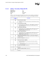
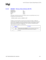
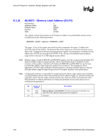
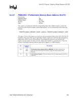
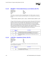
Host-PCI Express* Graphics Bridge Registers (D1:F0) R 8.1.16 MLIMIT1-Memory Limit Address (D1:F0) PCI Device: Address Offset: Default Value: Access: Size: 1 22h 0000h R/W 16 bits This register controls the processor-to-PCI Express Graphics non-prefetchable memory access routing based on the following formula: MEMORY_BASE ≤ address ≤ MEMORY_LIMIT The upper 12 bits of the register are read/write and correspond to the upper 12 address bits A[31:20] of the 32-bit address. The bottom 4 bits of this register are read-only and return zeroes when read. Configuration software must initialize this register. For the purpose of address decode, address bits A[19:0] are assumed to be FFFFFh. Thus, the top of the defined memory address range will be at the top of a 1-MB aligned memory block. Note: Memory range covered by MBASE and MLIMIT registers are used to map non-pre-fetchable PCI Express Graphics address ranges (typically, where control/status memory-mapped I/O data structures of the graphics controller will reside) and PMBASE and PMLIMIT are used to map pre-fetchable address ranges (typically, graphics local memory). This segregation allows application of USWC space attribute to be performed in a true plug-and-play manner to the prefetchable address range for improved processor-PCI Express memory access performance. Note: Configuration software is responsible for programming all address range registers (pre-fetchable, non-prefetchable) with the values that provide exclusive address ranges (i.e., prevent overlap with each other and/or with the ranges covered with the main memory). There is no provision in the MCH hardware to enforce prevention of overlap and operations of the system in the case of overlap are not guaranteed. Bit Access & Default Description 15:4 R/W Memory Address Limit (MLIMIT): This field corresponds to A[31:20] of the 000h upper limit of the address range passed to PCI Express*. 3:0 Reserved 122 Intel® 82925X/82925XE MCH Datasheet
-
 1
1 -
2
-
3
-
4
-
5
-
6
-
7
-
8
-
9
-
10
-
11
-
12
-
13
-
14
-
15
-
16
-
17
-
18
-
19
-
20
-
21
-
22
-
23
-
24
-
25
-
26
-
27
-
28
-
29
-
30
-
31
-
32
-
33
-
34
-
35
-
36
-
37
-
38
-
39
-
40
-
41
-
42
-
43
-
44
-
45
-
46
-
47
-
48
-
49
-
50
-
51
-
52
-
53
-
54
-
55
-
56
-
57
-
58
-
59
-
60
-
61
-
62
-
63
-
64
-
65
-
66
-
67
-
68
-
69
-
70
-
71
-
72
-
73
-
74
-
75
-
76
-
77
-
78
-
79
-
80
-
81
-
82
-
83
-
84
-
85
-
86
-
87
-
88
-
89
-
90
-
91
-
92
-
93
-
94
-
95
-
96
-
97
-
98
-
99
-
100
-
101
-
102
-
103
-
104
-
105
-
106
-
107
-
108
-
109
-
110
-
111
-
112
-
113
-
114
-
115
-
116
-
 117
117 -
 118
118 -
 119
119 -
 120
120 -
 121
121 -
 122
122 -
 123
123 -
 124
124 -
 125
125 -
 126
126 -
 127
127 -
128
-
129
-
130
-
131
-
132
-
133
-
134
-
135
-
136
-
137
-
138
-
139
-
140
-
141
-
142
-
143
-
144
-
145
-
146
-
147
-
148
-
149
-
150
-
151
-
152
-
153
-
154
-
155
-
156
-
157
-
158
-
159
-
160
-
161
-
162
-
163
-
164
-
165
-
166
-
167
-
168
-
169
-
170
-
171
-
172
-
173
-
174
-
175
-
176
-
177
-
178
-
179
-
180
-
181
-
182
-
183
-
184
-
185
-
186
-
187
-
188
-
189
-
190
-
191
-
192
-
193
-
194
-
195
-
196
-
197
-
198
-
199
-
200
-
201
-
202
-
203
-
204
-
205
-
206
-
207
-
208
-
209
-
210
-
211
-
212
-
213
-
214
-
215
-
216
-
217
-
218
-
219
-
220
-
221
-
222
-
223
-
224
-
225
-
226
-
227
-
228
-
229
-
230
-
231
-
232
-
233
-
234
-
235
-
236
-
237
-
238
-
239
-
240
-
241
-
242
 |
 |