Intel 925 Data Sheet - Page 127
ISA Enable ISAEN, SERR Enable SERREN, Parity Error Response Enable PEREN, cannot, ERR_COR
 |
UPC - 683728067724
View all Intel 925 manuals
Add to My Manuals
Save this manual to your list of manuals |
Page 127 highlights
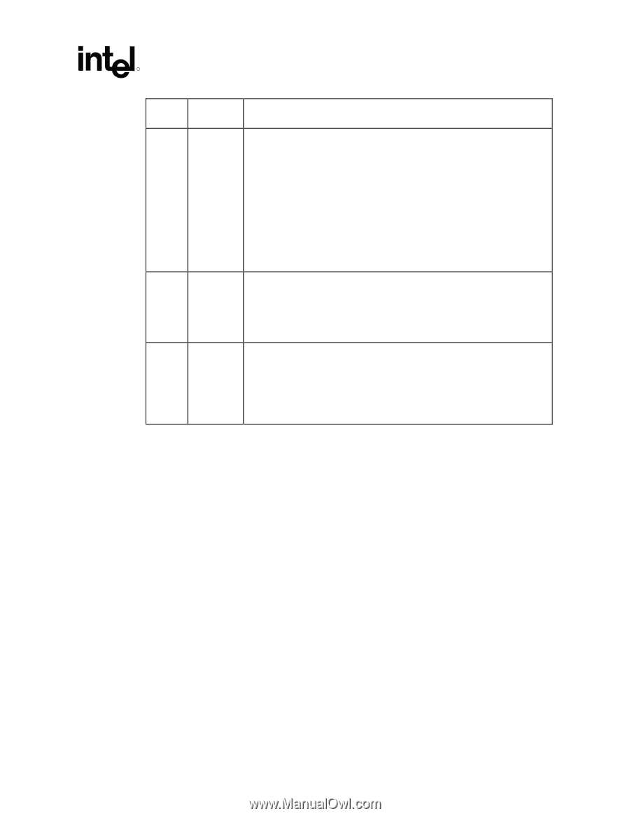
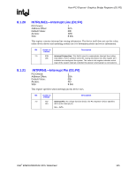
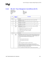
Host-PCI Express* Graphics Bridge Registers (D1:F0) R Bit Access & Default Description 2 R/W ISA Enable (ISAEN): This bit is needed to exclude legacy resource decode to 0b route ISA resources to legacy decode path. This bit modifies the response by the MCH to an I/O access issued by the processor that target ISA I/O addresses. This applies only to I/O addresses that are enabled by the IOBASE and IOLIMIT registers. 0 = All addresses defined by the IOBASE and IOLIMIT for processor I/O transactions will be mapped to PCI Express Graphics. 1 = MCH will not forward to PCI Express Graphics any I/O transactions addressing the last 768 bytes in each 1-KB block, even if the addresses are within the range defined by the IOBASE and IOLIMIT registers. Instead of going to PCI Express Graphics, these cycles are forwarded to DMI where they can be subtractively or positively claimed by the ISA bridge. 1 R/W SERR Enable (SERREN) 0b 0 = No forwarding of error messages from secondary side to primary side that could result in an SERR. 1 = ERR_COR, ERR_NONFATAL, and ERR_FATAL messages result in SERR message when individually enabled by the Root Control register. 0 RO Parity Error Response Enable (PEREN): This bit controls whether or not the 0b Master Data Parity Error bit in the Secondary Status register is set when the MCH receives across the link (upstream) a Read Data Completion Poisoned TLP. 0 = Master Data Parity Error bit in Secondary Status register cannot be set. 1 = Master Data Parity Error bit in Secondary Status register can be set.. Intel® 82925X/82925XE MCH Datasheet 127
-
 1
1 -
2
-
3
-
4
-
5
-
6
-
7
-
8
-
9
-
10
-
11
-
12
-
13
-
14
-
15
-
16
-
17
-
18
-
19
-
20
-
21
-
22
-
23
-
24
-
25
-
26
-
27
-
28
-
29
-
30
-
31
-
32
-
33
-
34
-
35
-
36
-
37
-
38
-
39
-
40
-
41
-
42
-
43
-
44
-
45
-
46
-
47
-
48
-
49
-
50
-
51
-
52
-
53
-
54
-
55
-
56
-
57
-
58
-
59
-
60
-
61
-
62
-
63
-
64
-
65
-
66
-
67
-
68
-
69
-
70
-
71
-
72
-
73
-
74
-
75
-
76
-
77
-
78
-
79
-
80
-
81
-
82
-
83
-
84
-
85
-
86
-
87
-
88
-
89
-
90
-
91
-
92
-
93
-
94
-
95
-
96
-
97
-
98
-
99
-
100
-
101
-
102
-
103
-
104
-
105
-
106
-
107
-
108
-
109
-
110
-
111
-
112
-
113
-
114
-
115
-
116
-
117
-
118
-
119
-
120
-
121
-
 122
122 -
 123
123 -
 124
124 -
 125
125 -
 126
126 -
 127
127 -
 128
128 -
 129
129 -
 130
130 -
 131
131 -
 132
132 -
133
-
134
-
135
-
136
-
137
-
138
-
139
-
140
-
141
-
142
-
143
-
144
-
145
-
146
-
147
-
148
-
149
-
150
-
151
-
152
-
153
-
154
-
155
-
156
-
157
-
158
-
159
-
160
-
161
-
162
-
163
-
164
-
165
-
166
-
167
-
168
-
169
-
170
-
171
-
172
-
173
-
174
-
175
-
176
-
177
-
178
-
179
-
180
-
181
-
182
-
183
-
184
-
185
-
186
-
187
-
188
-
189
-
190
-
191
-
192
-
193
-
194
-
195
-
196
-
197
-
198
-
199
-
200
-
201
-
202
-
203
-
204
-
205
-
206
-
207
-
208
-
209
-
210
-
211
-
212
-
213
-
214
-
215
-
216
-
217
-
218
-
219
-
220
-
221
-
222
-
223
-
224
-
225
-
226
-
227
-
228
-
229
-
230
-
231
-
232
-
233
-
234
-
235
-
236
-
237
-
238
-
239
-
240
-
241
-
242
 |
 |