Intel 925 Data Sheet - Page 138
LCAP-Link Capabilities D1:F0
 |
UPC - 683728067724
View all Intel 925 manuals
Add to My Manuals
Save this manual to your list of manuals |
Page 138 highlights
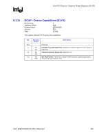
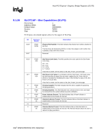
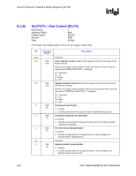
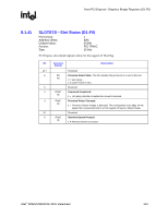
Host-PCI Express* Graphics Bridge Registers (D1:F0) R 8.1.36 LCAP-Link Capabilities (D1:F0) PCI Device: Address Offset: Default Value: Access: Size: 1 ACh 02012E01h R/WO 16 bits This register indicates PCI Express device specific capabilities. Bit 31:24 23:18 17:15 14:12 11:10 9:4 3:0 Access & Default Description RO 02h R/WO 010b R/WO 010b R/WO 11b RO 10h RO 1h Port Number: This field indicates the PCI Express* port number for the given PCI Express link. This field matches the value in Element Self Description [31:24]. Reserved L1 Exit Latency: This field indicates the length of time this Port requires to complete the transition from L1 to L0. The value 010 b indicates the range of 2 µs to less than 4 µs. If this field is required to be any value other than the default, BIOS must initialize it accordingly. Both bytes of this register that contain a portion of this field must be written simultaneously in order to prevent an intermediate (and undesired) value from ever existing. L0s Exit Latency: This field indicates the length of time this Port requires to complete the transition from L0s to L0. The value 010 b indicates the range of 128 ns to less than 256 ns. If this field is required to be any value other than the default, BIOS must initialize it accordingly. Note: When PCI Express* is operating with separate reference clocks, L0s exit latency may be greater than the setting in the L0s Exit Latency Register. Expect longer exit latency then setting in L0s Exit Latency Register. The link may enter Recovery state before reaching L0. System BIOS can program the appropriate Exit Latency and advertised N_FTS value if it detects that the downstream device is not using the common reference clock (indicated in the Slot Clock Configuration bit 12 of the device's Link Status Register) Active State Link PM Support: L0s and L1 entry supported. Max Link Width: Hardwired to indicate X16. When Force X1 mode is enabled on this PCI Express* x16 Graphics Interface device, this field reflects X1 (01h). Max Link Speed: Hardwired to indicate 2.5 Gb/s. 138 Intel® 82925X/82925XE MCH Datasheet
-
 1
1 -
2
-
3
-
4
-
5
-
6
-
7
-
8
-
9
-
10
-
11
-
12
-
13
-
14
-
15
-
16
-
17
-
18
-
19
-
20
-
21
-
22
-
23
-
24
-
25
-
26
-
27
-
28
-
29
-
30
-
31
-
32
-
33
-
34
-
35
-
36
-
37
-
38
-
39
-
40
-
41
-
42
-
43
-
44
-
45
-
46
-
47
-
48
-
49
-
50
-
51
-
52
-
53
-
54
-
55
-
56
-
57
-
58
-
59
-
60
-
61
-
62
-
63
-
64
-
65
-
66
-
67
-
68
-
69
-
70
-
71
-
72
-
73
-
74
-
75
-
76
-
77
-
78
-
79
-
80
-
81
-
82
-
83
-
84
-
85
-
86
-
87
-
88
-
89
-
90
-
91
-
92
-
93
-
94
-
95
-
96
-
97
-
98
-
99
-
100
-
101
-
102
-
103
-
104
-
105
-
106
-
107
-
108
-
109
-
110
-
111
-
112
-
113
-
114
-
115
-
116
-
117
-
118
-
119
-
120
-
121
-
122
-
123
-
124
-
125
-
126
-
127
-
128
-
129
-
130
-
131
-
132
-
 133
133 -
 134
134 -
 135
135 -
 136
136 -
 137
137 -
 138
138 -
 139
139 -
 140
140 -
 141
141 -
 142
142 -
 143
143 -
144
-
145
-
146
-
147
-
148
-
149
-
150
-
151
-
152
-
153
-
154
-
155
-
156
-
157
-
158
-
159
-
160
-
161
-
162
-
163
-
164
-
165
-
166
-
167
-
168
-
169
-
170
-
171
-
172
-
173
-
174
-
175
-
176
-
177
-
178
-
179
-
180
-
181
-
182
-
183
-
184
-
185
-
186
-
187
-
188
-
189
-
190
-
191
-
192
-
193
-
194
-
195
-
196
-
197
-
198
-
199
-
200
-
201
-
202
-
203
-
204
-
205
-
206
-
207
-
208
-
209
-
210
-
211
-
212
-
213
-
214
-
215
-
216
-
217
-
218
-
219
-
220
-
221
-
222
-
223
-
224
-
225
-
226
-
227
-
228
-
229
-
230
-
231
-
232
-
233
-
234
-
235
-
236
-
237
-
238
-
239
-
240
-
241
-
242
 |
 |