Intel 925 Data Sheet - Page 149
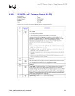
VC0RCAP-VC0 Resource Capability D1:F0, VC0RCTL-VC0 Resource Control D1:F0
 |
UPC - 683728067724
View all Intel 925 manuals
Add to My Manuals
Save this manual to your list of manuals |
Page 149 highlights
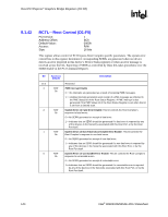
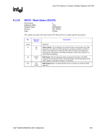
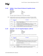
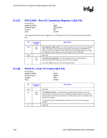
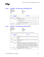
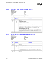
Host-PCI Express* Graphics Bridge Registers (D1:F0) R 8.1.49 VC0RCAP-VC0 Resource Capability (D1:F0) PCI Device: Address Offset: Default Value: Access: Size: 1 110h 00000000h RO 32 bits Bit 31:16 15 14:0 Access & Default Description Reserved RO Reject Snoop Transactions 0b 0 = Transactions with or without the No Snoop bit set within the TLP header are allowed on this VC. 1 = Any transaction without the No Snoop bit set within the TLP header will be rejected as an Unsupported Request. Reserved 8.1.50 VC0RCTL-VC0 Resource Control (D1:F0) PCI Device: Address Offset: Default Value: Access: Size: 1 114h 8000007Fh RO, R/W 32 bits This register controls the resources associated with PCI Express Virtual Channel 0. Bit 31 30:27 26:24 23:8 7:1 0 Access & Default Description RO 1b RO 000b R/W 7Fh RO 1b VC0 Enable: For VC0 this is hardwired to 1 and read only as VC0 can never be disabled. Reserved VC0 ID: This field assigns a VC ID to the VC resource. For VC0 this is hardwired to 0 and read only. Reserved TC/VC0 Map: This field indicates the TCs (Traffic Classes) that are mapped to the VC resource. Bit locations within this field correspond to TC values. For example, when bit 7 is set in this field, TC7 is mapped to this VC resource. When more than one bit in this field is set, it indicates that multiple TCs are mapped to the VC resource. In order to remove one or more TCs from the TC/VC Map of an enabled VC, software must ensure that no new or outstanding transactions with the TC labels are targeted at the given Link. TC0/VC0 Map: Traffic Class 0 is always routed to VC0. Intel® 82925X/82925XE MCH Datasheet 149
-
 1
1 -
2
-
3
-
4
-
5
-
6
-
7
-
8
-
9
-
10
-
11
-
12
-
13
-
14
-
15
-
16
-
17
-
18
-
19
-
20
-
21
-
22
-
23
-
24
-
25
-
26
-
27
-
28
-
29
-
30
-
31
-
32
-
33
-
34
-
35
-
36
-
37
-
38
-
39
-
40
-
41
-
42
-
43
-
44
-
45
-
46
-
47
-
48
-
49
-
50
-
51
-
52
-
53
-
54
-
55
-
56
-
57
-
58
-
59
-
60
-
61
-
62
-
63
-
64
-
65
-
66
-
67
-
68
-
69
-
70
-
71
-
72
-
73
-
74
-
75
-
76
-
77
-
78
-
79
-
80
-
81
-
82
-
83
-
84
-
85
-
86
-
87
-
88
-
89
-
90
-
91
-
92
-
93
-
94
-
95
-
96
-
97
-
98
-
99
-
100
-
101
-
102
-
103
-
104
-
105
-
106
-
107
-
108
-
109
-
110
-
111
-
112
-
113
-
114
-
115
-
116
-
117
-
118
-
119
-
120
-
121
-
122
-
123
-
124
-
125
-
126
-
127
-
128
-
129
-
130
-
131
-
132
-
133
-
134
-
135
-
136
-
137
-
138
-
139
-
140
-
141
-
142
-
143
-
 144
144 -
 145
145 -
 146
146 -
 147
147 -
 148
148 -
 149
149 -
 150
150 -
 151
151 -
 152
152 -
 153
153 -
 154
154 -
155
-
156
-
157
-
158
-
159
-
160
-
161
-
162
-
163
-
164
-
165
-
166
-
167
-
168
-
169
-
170
-
171
-
172
-
173
-
174
-
175
-
176
-
177
-
178
-
179
-
180
-
181
-
182
-
183
-
184
-
185
-
186
-
187
-
188
-
189
-
190
-
191
-
192
-
193
-
194
-
195
-
196
-
197
-
198
-
199
-
200
-
201
-
202
-
203
-
204
-
205
-
206
-
207
-
208
-
209
-
210
-
211
-
212
-
213
-
214
-
215
-
216
-
217
-
218
-
219
-
220
-
221
-
222
-
223
-
224
-
225
-
226
-
227
-
228
-
229
-
230
-
231
-
232
-
233
-
234
-
235
-
236
-
237
-
238
-
239
-
240
-
241
-
242
 |
 |