Intel 925 Data Sheet - Page 154
LE1D-Link Entry 1 Description D1:F0
 |
UPC - 683728067724
View all Intel 925 manuals
Add to My Manuals
Save this manual to your list of manuals |
Page 154 highlights
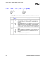
Host-PCI Express* Graphics Bridge Registers (D1:F0) R 8.1.57 LE1D-Link Entry 1 Description (D1:F0) PCI Device: Address Offset: Default Value: Access: Size: 1 150h 00000000h RO, R/WO 32 bits This register provides the First part of a Link Entry that declares an internal link to another Root Complex Element. Bit 31:24 23:16 15:2 1 0 Access & Default Description RO 00h R/WO 00h RO 0b R/WO 0b Target Port Number: This field specifies the port number associated with the element targeted by this link entry (Egress Port). The target port number is with respect to the component that contains this element as specified by the target component ID. Target Component ID: This field indicates the physical or logical component that is targeted by this link entry. A value of 0 is reserved; Component IDs start at 1. This value is a mirror of the value in the Component ID field of all elements in this component. The value only needs to be written in one of the mirrored fields and it will be reflected everywhere that it is mirrored. Reserved Link Type: This field indicates that the link points to memory-mapped space (for RCRB). The link address specifies the 64-bit base address of the target RCRB. Link Valid: 0 = Link Entry is not valid and will be ignored. 1 = Link Entry specifies a valid link. 154 Intel® 82925X/82925XE MCH Datasheet
-
 1
1 -
2
-
3
-
4
-
5
-
6
-
7
-
8
-
9
-
10
-
11
-
12
-
13
-
14
-
15
-
16
-
17
-
18
-
19
-
20
-
21
-
22
-
23
-
24
-
25
-
26
-
27
-
28
-
29
-
30
-
31
-
32
-
33
-
34
-
35
-
36
-
37
-
38
-
39
-
40
-
41
-
42
-
43
-
44
-
45
-
46
-
47
-
48
-
49
-
50
-
51
-
52
-
53
-
54
-
55
-
56
-
57
-
58
-
59
-
60
-
61
-
62
-
63
-
64
-
65
-
66
-
67
-
68
-
69
-
70
-
71
-
72
-
73
-
74
-
75
-
76
-
77
-
78
-
79
-
80
-
81
-
82
-
83
-
84
-
85
-
86
-
87
-
88
-
89
-
90
-
91
-
92
-
93
-
94
-
95
-
96
-
97
-
98
-
99
-
100
-
101
-
102
-
103
-
104
-
105
-
106
-
107
-
108
-
109
-
110
-
111
-
112
-
113
-
114
-
115
-
116
-
117
-
118
-
119
-
120
-
121
-
122
-
123
-
124
-
125
-
126
-
127
-
128
-
129
-
130
-
131
-
132
-
133
-
134
-
135
-
136
-
137
-
138
-
139
-
140
-
141
-
142
-
143
-
144
-
145
-
146
-
147
-
148
-
 149
149 -
 150
150 -
 151
151 -
 152
152 -
 153
153 -
 154
154 -
 155
155 -
 156
156 -
 157
157 -
 158
158 -
 159
159 -
160
-
161
-
162
-
163
-
164
-
165
-
166
-
167
-
168
-
169
-
170
-
171
-
172
-
173
-
174
-
175
-
176
-
177
-
178
-
179
-
180
-
181
-
182
-
183
-
184
-
185
-
186
-
187
-
188
-
189
-
190
-
191
-
192
-
193
-
194
-
195
-
196
-
197
-
198
-
199
-
200
-
201
-
202
-
203
-
204
-
205
-
206
-
207
-
208
-
209
-
210
-
211
-
212
-
213
-
214
-
215
-
216
-
217
-
218
-
219
-
220
-
221
-
222
-
223
-
224
-
225
-
226
-
227
-
228
-
229
-
230
-
231
-
232
-
233
-
234
-
235
-
236
-
237
-
238
-
239
-
240
-
241
-
242
 |
 |