Intel 925 Data Sheet - Page 158
Legacy Address Range, System Address Ranges
 |
UPC - 683728067724
View all Intel 925 manuals
Add to My Manuals
Save this manual to your list of manuals |
Page 158 highlights
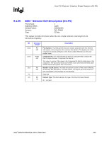
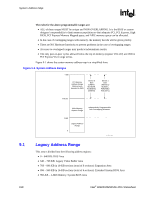
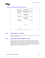
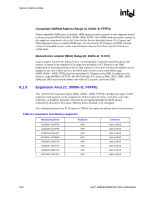
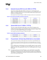
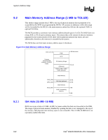
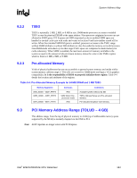
System Address Map R The rules for the above programmable ranges are: • ALL of these ranges MUST be unique and NON-OVERLAPPING. It is the BIOS or system designer's responsibility to limit memory population so that adequate PCI, PCI Express, High BIOS, PCI Express Memory Mapped space, and APIC memory space can be allocated. • In the case of overlapping ranges with memory, the memory decode will be given priority. • There are NO Hardware Interlocks to prevent problems in the case of overlapping ranges. • Accesses to overlapped ranges may produce indeterminate results. • The only peer-to-peer cycles allowed below the top of memory (register TOLUD) are DMI to PCI Express VGA range writes. Figure 9-1 shows the system memory address map in a simplified form. Figure 9-1. System Address Ranges 4 GB PCI Memory Address Range (Subtractively decoded to DMI) Device 0 Bars (EPBAR, MCHBAR, PCIEXBAR, DMIBAR) Device 1 Bars (MBASE1/ MLIMIT1, PMBASE1/ PMLIMIT1) TOLUD Main Memory Address Range Independently Programmable Non-Overlapping Windows 1 MB Legacy Address Range 0 Sys_Address_Ranges 9.1 Legacy Address Range This area is divided into the following address regions: • 0 - 640 KB: DOS Area • 640 - 768 KB: Legacy Video Buffer Area • 768 - 896 KB in 16-KB sections (total of 8 sections): Expansion Area • 896 - 960 KB in 16-KB sections (total of 4 sections): Extended System BIOS Area • 960-KB - 1-MB Memory: System BIOS Area 158 Intel® 82925X/82925XE MCH Datasheet
-
 1
1 -
2
-
3
-
4
-
5
-
6
-
7
-
8
-
9
-
10
-
11
-
12
-
13
-
14
-
15
-
16
-
17
-
18
-
19
-
20
-
21
-
22
-
23
-
24
-
25
-
26
-
27
-
28
-
29
-
30
-
31
-
32
-
33
-
34
-
35
-
36
-
37
-
38
-
39
-
40
-
41
-
42
-
43
-
44
-
45
-
46
-
47
-
48
-
49
-
50
-
51
-
52
-
53
-
54
-
55
-
56
-
57
-
58
-
59
-
60
-
61
-
62
-
63
-
64
-
65
-
66
-
67
-
68
-
69
-
70
-
71
-
72
-
73
-
74
-
75
-
76
-
77
-
78
-
79
-
80
-
81
-
82
-
83
-
84
-
85
-
86
-
87
-
88
-
89
-
90
-
91
-
92
-
93
-
94
-
95
-
96
-
97
-
98
-
99
-
100
-
101
-
102
-
103
-
104
-
105
-
106
-
107
-
108
-
109
-
110
-
111
-
112
-
113
-
114
-
115
-
116
-
117
-
118
-
119
-
120
-
121
-
122
-
123
-
124
-
125
-
126
-
127
-
128
-
129
-
130
-
131
-
132
-
133
-
134
-
135
-
136
-
137
-
138
-
139
-
140
-
141
-
142
-
143
-
144
-
145
-
146
-
147
-
148
-
149
-
150
-
151
-
152
-
 153
153 -
 154
154 -
 155
155 -
 156
156 -
 157
157 -
 158
158 -
 159
159 -
 160
160 -
 161
161 -
 162
162 -
 163
163 -
164
-
165
-
166
-
167
-
168
-
169
-
170
-
171
-
172
-
173
-
174
-
175
-
176
-
177
-
178
-
179
-
180
-
181
-
182
-
183
-
184
-
185
-
186
-
187
-
188
-
189
-
190
-
191
-
192
-
193
-
194
-
195
-
196
-
197
-
198
-
199
-
200
-
201
-
202
-
203
-
204
-
205
-
206
-
207
-
208
-
209
-
210
-
211
-
212
-
213
-
214
-
215
-
216
-
217
-
218
-
219
-
220
-
221
-
222
-
223
-
224
-
225
-
226
-
227
-
228
-
229
-
230
-
231
-
232
-
233
-
234
-
235
-
236
-
237
-
238
-
239
-
240
-
241
-
242
 |
 |