Intel 925 Data Sheet - Page 160
Expansion Area C_0000h-D_FFFFh, Compatible SMRAM Address Range A_0000h-B_FFFFh
 |
UPC - 683728067724
View all Intel 925 manuals
Add to My Manuals
Save this manual to your list of manuals |
Page 160 highlights
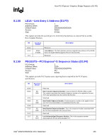
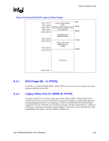
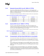
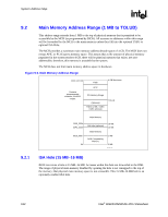
System Address Map R Compatible SMRAM Address Range (A_0000h-B_FFFFh) When compatible SMM space is enabled, SMM-mode processor accesses to this range are routed to physical system DRAM at 000A_0000h-000B_FFFFh. Non-SMM-mode processor accesses to this range are considered to be to the Video Buffer Area as described above. PCI Express and DMI originated cycles to enabled SMM space are not allowed. PCI Express and DMI initiated cycles are attempted as peer cycles, and will master abort on PCI if no external VGA device claims them. Monochrome Adapter (MDA) Range (B_0000h-B_7FFFh) Legacy support requires the ability to have a second graphics controller (monochrome) in the system. Accesses in the standard VGA range are forwarded to PCI Express or the DMI (depending on the programming of the on-chip registers). Since the monochrome adapter may be mapped to any one of these devices, the MCH must decode cycles in the MDA range (000B_0000h - 000B_7FFFh) and forward either PCI Express or the DMI. In addition to the memory range B0000h to B7FFFh, the MCH decodes I/O cycles at 3B4h, 3B5h, 3B8h, 3B9h, 3BAh and 3BFh and forwards them to the either PCI Express, and/or the DMI. 9.1.3 Expansion Area (C_0000h-D_FFFFh) This 128-KB ISA Expansion region (000C_0000h - 000D_FFFFh) is divided into eight, 16-KB segments. Each segment can be assigned one of four read/write states: read only, write only, read/write, or disabled. Typically, these blocks are mapped through the MCH and are subtractively decoded to ISA space. Memory that is disabled is not remapped. Non-snooped accesses from PCI Express or DMI to this region are always sent to main memory. Table 9-1. Expansion Area Memory Segments Memory Segments 0C0000h-0C3FFFh 0C4000h-0C7FFFh 0C8000h-0CBFFFh 0CC000h -0CFFFFh 0D0000h-0D3FFFh 0D4000h-0D7FFFh 0D8000h-0DBFFFh 0DC000h-0DFFFFh Attributes W/R W/R W/R W/R W/R W/R W/R W/R Comments Add-on BIOS Add-on BIOS Add-on BIOS Add-on BIOS Add-on BIOS Add-on BIOS Add-on BIOS Add-on BIOS 160 Intel® 82925X/82925XE MCH Datasheet
-
 1
1 -
2
-
3
-
4
-
5
-
6
-
7
-
8
-
9
-
10
-
11
-
12
-
13
-
14
-
15
-
16
-
17
-
18
-
19
-
20
-
21
-
22
-
23
-
24
-
25
-
26
-
27
-
28
-
29
-
30
-
31
-
32
-
33
-
34
-
35
-
36
-
37
-
38
-
39
-
40
-
41
-
42
-
43
-
44
-
45
-
46
-
47
-
48
-
49
-
50
-
51
-
52
-
53
-
54
-
55
-
56
-
57
-
58
-
59
-
60
-
61
-
62
-
63
-
64
-
65
-
66
-
67
-
68
-
69
-
70
-
71
-
72
-
73
-
74
-
75
-
76
-
77
-
78
-
79
-
80
-
81
-
82
-
83
-
84
-
85
-
86
-
87
-
88
-
89
-
90
-
91
-
92
-
93
-
94
-
95
-
96
-
97
-
98
-
99
-
100
-
101
-
102
-
103
-
104
-
105
-
106
-
107
-
108
-
109
-
110
-
111
-
112
-
113
-
114
-
115
-
116
-
117
-
118
-
119
-
120
-
121
-
122
-
123
-
124
-
125
-
126
-
127
-
128
-
129
-
130
-
131
-
132
-
133
-
134
-
135
-
136
-
137
-
138
-
139
-
140
-
141
-
142
-
143
-
144
-
145
-
146
-
147
-
148
-
149
-
150
-
151
-
152
-
153
-
154
-
 155
155 -
 156
156 -
 157
157 -
 158
158 -
 159
159 -
 160
160 -
 161
161 -
 162
162 -
 163
163 -
 164
164 -
 165
165 -
166
-
167
-
168
-
169
-
170
-
171
-
172
-
173
-
174
-
175
-
176
-
177
-
178
-
179
-
180
-
181
-
182
-
183
-
184
-
185
-
186
-
187
-
188
-
189
-
190
-
191
-
192
-
193
-
194
-
195
-
196
-
197
-
198
-
199
-
200
-
201
-
202
-
203
-
204
-
205
-
206
-
207
-
208
-
209
-
210
-
211
-
212
-
213
-
214
-
215
-
216
-
217
-
218
-
219
-
220
-
221
-
222
-
223
-
224
-
225
-
226
-
227
-
228
-
229
-
230
-
231
-
232
-
233
-
234
-
235
-
236
-
237
-
238
-
239
-
240
-
241
-
242
 |
 |