Intel 925 Data Sheet - Page 163
PCI Memory Address Range TOLUD - 4 GB, Pre-allocated Memory
 |
UPC - 683728067724
View all Intel 925 manuals
Add to My Manuals
Save this manual to your list of manuals |
Page 163 highlights
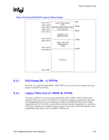
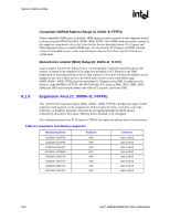
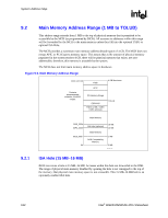
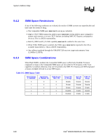
System Address Map R 9.2.2 TSEG TSEG is optionally 1 MB, 2 MB, or 8 MB in size. SMM-mode processor accesses to enabled TSEG access the physical DRAM at the same address. Non-processor originated accesses are not allowed to SMM space. PCI Express and DMI originated cycles to enabled SMM space are handled as invalid cycle type with reads and writes to location 0 and byte enables turned off for writes. When the extended SMRAM space is enabled, processor accesses to the TSEG range without SMM attribute or without WB attribute are also forwarded to memory as invalid accesses. Non-SMM-mode write-back cycles that target TSEG space are completed to main memory for cache coherency. When SMM is enabled, the maximum amount of memory available to the system is equal to the amount of physical main memory minus the value in the TSEG register which is fixed at 1 MB, 2 MB, or 8 MB. 9.2.3 Pre-allocated Memory Voids of physical addresses that are not accessible as general system memory and reside within system memory address range (< TOLUD) are created for SMM-mode and legacy VGA graphics compatibility. It is the responsibility of BIOS to properly initialize these regions. Table 9-4 details the location and attributes of the regions. Table 9-4. Pre-Allocated Memory Example for 64-MB DRAM and 1-MB TSEG Memory Segments 0000_0000h - 03DF_FFFFh 03E0_0000h - 03EF_FFFFh 03F0_0000h - 03FF_FFFFh Attributes R/W SMM Mode Only processor reads R/W Comments Available system memory 62 MB TSEG Address Range and Pre-allocated memory Pre-allocated Graphics VGA memory. 9.3 PCI Memory Address Range (TOLUD - 4 GB) This address range, from the top of physical memory to 4 GB (top of addressable memory space supported by the MCH) is normally mapped via the DMI to PCI. Note: AGIP Aperture no longer exists with PCI Express. Intel® 82925X/82925XE MCH Datasheet 163
-
 1
1 -
2
-
3
-
4
-
5
-
6
-
7
-
8
-
9
-
10
-
11
-
12
-
13
-
14
-
15
-
16
-
17
-
18
-
19
-
20
-
21
-
22
-
23
-
24
-
25
-
26
-
27
-
28
-
29
-
30
-
31
-
32
-
33
-
34
-
35
-
36
-
37
-
38
-
39
-
40
-
41
-
42
-
43
-
44
-
45
-
46
-
47
-
48
-
49
-
50
-
51
-
52
-
53
-
54
-
55
-
56
-
57
-
58
-
59
-
60
-
61
-
62
-
63
-
64
-
65
-
66
-
67
-
68
-
69
-
70
-
71
-
72
-
73
-
74
-
75
-
76
-
77
-
78
-
79
-
80
-
81
-
82
-
83
-
84
-
85
-
86
-
87
-
88
-
89
-
90
-
91
-
92
-
93
-
94
-
95
-
96
-
97
-
98
-
99
-
100
-
101
-
102
-
103
-
104
-
105
-
106
-
107
-
108
-
109
-
110
-
111
-
112
-
113
-
114
-
115
-
116
-
117
-
118
-
119
-
120
-
121
-
122
-
123
-
124
-
125
-
126
-
127
-
128
-
129
-
130
-
131
-
132
-
133
-
134
-
135
-
136
-
137
-
138
-
139
-
140
-
141
-
142
-
143
-
144
-
145
-
146
-
147
-
148
-
149
-
150
-
151
-
152
-
153
-
154
-
155
-
156
-
157
-
 158
158 -
 159
159 -
 160
160 -
 161
161 -
 162
162 -
 163
163 -
 164
164 -
 165
165 -
 166
166 -
 167
167 -
 168
168 -
169
-
170
-
171
-
172
-
173
-
174
-
175
-
176
-
177
-
178
-
179
-
180
-
181
-
182
-
183
-
184
-
185
-
186
-
187
-
188
-
189
-
190
-
191
-
192
-
193
-
194
-
195
-
196
-
197
-
198
-
199
-
200
-
201
-
202
-
203
-
204
-
205
-
206
-
207
-
208
-
209
-
210
-
211
-
212
-
213
-
214
-
215
-
216
-
217
-
218
-
219
-
220
-
221
-
222
-
223
-
224
-
225
-
226
-
227
-
228
-
229
-
230
-
231
-
232
-
233
-
234
-
235
-
236
-
237
-
238
-
239
-
240
-
241
-
242
 |
 |
