Intel 925 Data Sheet - Page 165
HSEG FEDA_0000h-FEDB_FFFFh, FSB Interrupt Memory Space FEE0_0000h-FEEF_FFFFh, High BIOS Area
 |
UPC - 683728067724
View all Intel 925 manuals
Add to My Manuals
Save this manual to your list of manuals |
Page 165 highlights
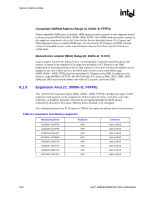
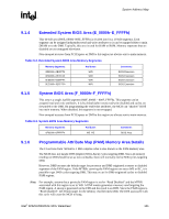
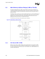
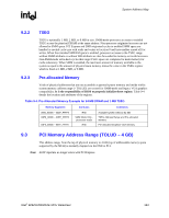
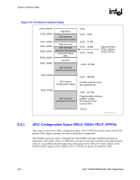
System Address Map R 9.3.2 9.3.3 9.3.4 9.3.5 HSEG (FEDA_0000h-FEDB_FFFFh) This optional segment from FEDA_0000h to FEDB_FFFFh provides a remapping window to SMM memory. It is sometimes called the High SMM memory space. SMM-mode processor accesses to the optionally enabled HSEG are remapped to 000A_0000h - 000B_FFFFh. NonSMM-mode processor accesses to enabled HSEG are considered invalid and are terminated immediately on the FSB. The exceptions to this rule are Non-SMM-mode write-back cycles that are remapped to SMM space to maintain cache coherency. PCI Express and DMI originated cycles to enabled SMM space are not allowed. Physical main memory behind the HSEG transaction address is not remapped and is not accessible. All cacheline writes with WB attribute or Implicit write backs to the HSEG range are completed to DRAM like an SMM cycle. FSB Interrupt Memory Space (FEE0_0000h-FEEF_FFFFh) The FSB Interrupt space is the address used to deliver interrupts to the FSB. Any device on PCI Express or DMI may issue a memory write to 0FEEx_xxxxh. The MCH will forward this memory write along with the data to the FSB as an Interrupt Message Transaction. The MCH terminates the FSB transaction by providing the response and asserting HTRDY#. This memory write cycle does not go to main memory. High BIOS Area The top 2 MB (FFE0_0000h - FFFF_FFFFh) of the PCI memory address range is reserved for system BIOS (High BIOS), extended BIOS for PCI devices, and the A20 alias of the system BIOS. The processor begins execution from the High BIOS after reset. This region is mapped to the DMI so that the upper subset of this region aliases to the 16-MB-256-KB range. The actual address space required for the BIOS is less than 2 MB, but the minimum processor MTRR range for this region is 2 MB; thus, that full 2 MB must be considered. PCI Express* Configuration Address Space A configuration register defines the base address for the 256-MB block of addresses below top of addressable memory (4 GB) for the configuration space associated with all devices and functions that are potentially a part of the PCI Express root complex hierarchy. This range will be aligned to a 256-MB boundary. BIOS must assign this address range such that it will not conflict with any other address ranges. Intel® 82925X/82925XE MCH Datasheet 165
-
 1
1 -
2
-
3
-
4
-
5
-
6
-
7
-
8
-
9
-
10
-
11
-
12
-
13
-
14
-
15
-
16
-
17
-
18
-
19
-
20
-
21
-
22
-
23
-
24
-
25
-
26
-
27
-
28
-
29
-
30
-
31
-
32
-
33
-
34
-
35
-
36
-
37
-
38
-
39
-
40
-
41
-
42
-
43
-
44
-
45
-
46
-
47
-
48
-
49
-
50
-
51
-
52
-
53
-
54
-
55
-
56
-
57
-
58
-
59
-
60
-
61
-
62
-
63
-
64
-
65
-
66
-
67
-
68
-
69
-
70
-
71
-
72
-
73
-
74
-
75
-
76
-
77
-
78
-
79
-
80
-
81
-
82
-
83
-
84
-
85
-
86
-
87
-
88
-
89
-
90
-
91
-
92
-
93
-
94
-
95
-
96
-
97
-
98
-
99
-
100
-
101
-
102
-
103
-
104
-
105
-
106
-
107
-
108
-
109
-
110
-
111
-
112
-
113
-
114
-
115
-
116
-
117
-
118
-
119
-
120
-
121
-
122
-
123
-
124
-
125
-
126
-
127
-
128
-
129
-
130
-
131
-
132
-
133
-
134
-
135
-
136
-
137
-
138
-
139
-
140
-
141
-
142
-
143
-
144
-
145
-
146
-
147
-
148
-
149
-
150
-
151
-
152
-
153
-
154
-
155
-
156
-
157
-
158
-
159
-
 160
160 -
 161
161 -
 162
162 -
 163
163 -
 164
164 -
 165
165 -
 166
166 -
 167
167 -
 168
168 -
 169
169 -
 170
170 -
171
-
172
-
173
-
174
-
175
-
176
-
177
-
178
-
179
-
180
-
181
-
182
-
183
-
184
-
185
-
186
-
187
-
188
-
189
-
190
-
191
-
192
-
193
-
194
-
195
-
196
-
197
-
198
-
199
-
200
-
201
-
202
-
203
-
204
-
205
-
206
-
207
-
208
-
209
-
210
-
211
-
212
-
213
-
214
-
215
-
216
-
217
-
218
-
219
-
220
-
221
-
222
-
223
-
224
-
225
-
226
-
227
-
228
-
229
-
230
-
231
-
232
-
233
-
234
-
235
-
236
-
237
-
238
-
239
-
240
-
241
-
242
 |
 |