Intel 925 Data Sheet - Page 166
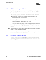
PCI Express* Graphics Attach, AGP DRAM Graphics Aperture
 |
UPC - 683728067724
View all Intel 925 manuals
Add to My Manuals
Save this manual to your list of manuals |
Page 166 highlights
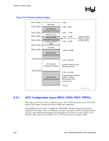
System Address Map R 9.3.6 PCI Express* Graphics Attach The MCH can be programmed to direct memory accesses to the PCI Express interface when addresses are within either of two programmed ranges specified via registers in the MCH's Device 1 configuration space. • The first range is controlled via the Memory Base Register (MBASE) and Memory Limit Register (MLIMIT) registers. • The second range is controlled via the Prefetchable Memory Base (PMBASE) and Prefetchable Memory Limit (PMLIMIT) registers. The MCH positively decodes memory accesses to PCI Express memory address space as defined by the following equations: Memory_Base_Address ≤ Address ≤ Memory_Limit_Address Prefetchable_Memory_Base_Address ≤ Address ≤ Prefetchable_Memory_Limit_Address It is essential to support a separate Prefetchable range to apply USWC attribute (from the processor point of view) to that range. The USWC attribute is used by the processor for write combining. Note: The programmable ranges are used to allocate memory address space for any PCI Express devices sitting on PCI Express that require such a window. The PCICMD1 register can override the routing of memory accesses to PCI Express. In other words, the memory access enable bit must be set in the device 1 PCICMD1 register to enable the memory base/limit and prefetchable base/limit windows. 9.3.7 AGP DRAM Graphics Aperture Unlike AGP4x, PCI Express has no concept of aperture for PCI Express devices. As a result, there is no need to translate addresses from PCI Express. Therefore, the MCH has no APBASE and APSIZE registers. 166 Intel® 82925X/82925XE MCH Datasheet
-
 1
1 -
2
-
3
-
4
-
5
-
6
-
7
-
8
-
9
-
10
-
11
-
12
-
13
-
14
-
15
-
16
-
17
-
18
-
19
-
20
-
21
-
22
-
23
-
24
-
25
-
26
-
27
-
28
-
29
-
30
-
31
-
32
-
33
-
34
-
35
-
36
-
37
-
38
-
39
-
40
-
41
-
42
-
43
-
44
-
45
-
46
-
47
-
48
-
49
-
50
-
51
-
52
-
53
-
54
-
55
-
56
-
57
-
58
-
59
-
60
-
61
-
62
-
63
-
64
-
65
-
66
-
67
-
68
-
69
-
70
-
71
-
72
-
73
-
74
-
75
-
76
-
77
-
78
-
79
-
80
-
81
-
82
-
83
-
84
-
85
-
86
-
87
-
88
-
89
-
90
-
91
-
92
-
93
-
94
-
95
-
96
-
97
-
98
-
99
-
100
-
101
-
102
-
103
-
104
-
105
-
106
-
107
-
108
-
109
-
110
-
111
-
112
-
113
-
114
-
115
-
116
-
117
-
118
-
119
-
120
-
121
-
122
-
123
-
124
-
125
-
126
-
127
-
128
-
129
-
130
-
131
-
132
-
133
-
134
-
135
-
136
-
137
-
138
-
139
-
140
-
141
-
142
-
143
-
144
-
145
-
146
-
147
-
148
-
149
-
150
-
151
-
152
-
153
-
154
-
155
-
156
-
157
-
158
-
159
-
160
-
 161
161 -
 162
162 -
 163
163 -
 164
164 -
 165
165 -
 166
166 -
 167
167 -
 168
168 -
 169
169 -
 170
170 -
 171
171 -
172
-
173
-
174
-
175
-
176
-
177
-
178
-
179
-
180
-
181
-
182
-
183
-
184
-
185
-
186
-
187
-
188
-
189
-
190
-
191
-
192
-
193
-
194
-
195
-
196
-
197
-
198
-
199
-
200
-
201
-
202
-
203
-
204
-
205
-
206
-
207
-
208
-
209
-
210
-
211
-
212
-
213
-
214
-
215
-
216
-
217
-
218
-
219
-
220
-
221
-
222
-
223
-
224
-
225
-
226
-
227
-
228
-
229
-
230
-
231
-
232
-
233
-
234
-
235
-
236
-
237
-
238
-
239
-
240
-
241
-
242
 |
 |