Intel 925 Data Sheet - Page 171
PCI Express* I/O Address Mapping, MCH Decode Rules and Cross-Bridge Address Mapping, Legacy VGA - processor pentium d
 |
UPC - 683728067724
View all Intel 925 manuals
Add to My Manuals
Save this manual to your list of manuals |
Page 171 highlights
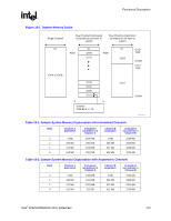
System Address Map R 9.4.10 9.4.11 9.4.12 The I/O accesses (other than ones used for configuration space access) are forwarded normally to the DMI bus unless they fall within the PCI Express I/O address range as defined by the mechanisms explained below. I/O writes are not posted. Memory writes to the ICH6 or PCI Express are posted. The MCH responds to I/O cycles initiated on PCI Express or DMI with a UR status. Upstream I/O cycles and configuration cycles should never occur. If one does occur, the request will route as a read to memory address 0h so a completion is naturally generated (whether the original request was a read or write). The transaction will complete with a UR completion status. For Pentium 4 processors, I/O reads that lie within 8-byte boundaries but cross 4-byte boundaries are issued from the processor as 1 transaction. The MCH will break this into 2 separate transactions. This has not been done on previous chipsets. I/O writes that lie within 8-byte boundaries but cross 4-byte boundaries are assumed to be split into 2 transactions by the processor. PCI Express* I/O Address Mapping The MCH can be programmed to direct non-memory (I/O) accesses to the PCI Express bus interface when processor-initiated I/O cycle addresses are within the PCI Express I/O address range. MCH Decode Rules and Cross-Bridge Address Mapping The following are MCH decode rules and cross-bridge address mapping used in this chipset: • VGAA = 000A_0000h - 000A_FFFFh • MDA = 000B_0000h - 000B_7FFFh • VGAB = 000B_8000h - 000B_FFFFh • MAINMEM = 0100_0000h to TOLUD Legacy VGA and I/O Range Decode Rules The legacy 128-KB VGA memory range 000A_0000h-000B_FFFFh can be mapped to PCI Express (Device 1), and/or to the DMI depending on BIOS programming. Priority for VGA mapping is constant in that the MCH always decodes internally mapped devices first. The MCH always positively decodes internally mapped devices, namely the PCI Express. § Intel® 82925X/82925XE MCH Datasheet 171
-
 1
1 -
2
-
3
-
4
-
5
-
6
-
7
-
8
-
9
-
10
-
11
-
12
-
13
-
14
-
15
-
16
-
17
-
18
-
19
-
20
-
21
-
22
-
23
-
24
-
25
-
26
-
27
-
28
-
29
-
30
-
31
-
32
-
33
-
34
-
35
-
36
-
37
-
38
-
39
-
40
-
41
-
42
-
43
-
44
-
45
-
46
-
47
-
48
-
49
-
50
-
51
-
52
-
53
-
54
-
55
-
56
-
57
-
58
-
59
-
60
-
61
-
62
-
63
-
64
-
65
-
66
-
67
-
68
-
69
-
70
-
71
-
72
-
73
-
74
-
75
-
76
-
77
-
78
-
79
-
80
-
81
-
82
-
83
-
84
-
85
-
86
-
87
-
88
-
89
-
90
-
91
-
92
-
93
-
94
-
95
-
96
-
97
-
98
-
99
-
100
-
101
-
102
-
103
-
104
-
105
-
106
-
107
-
108
-
109
-
110
-
111
-
112
-
113
-
114
-
115
-
116
-
117
-
118
-
119
-
120
-
121
-
122
-
123
-
124
-
125
-
126
-
127
-
128
-
129
-
130
-
131
-
132
-
133
-
134
-
135
-
136
-
137
-
138
-
139
-
140
-
141
-
142
-
143
-
144
-
145
-
146
-
147
-
148
-
149
-
150
-
151
-
152
-
153
-
154
-
155
-
156
-
157
-
158
-
159
-
160
-
161
-
162
-
163
-
164
-
165
-
 166
166 -
 167
167 -
 168
168 -
 169
169 -
 170
170 -
 171
171 -
 172
172 -
 173
173 -
 174
174 -
 175
175 -
 176
176 -
177
-
178
-
179
-
180
-
181
-
182
-
183
-
184
-
185
-
186
-
187
-
188
-
189
-
190
-
191
-
192
-
193
-
194
-
195
-
196
-
197
-
198
-
199
-
200
-
201
-
202
-
203
-
204
-
205
-
206
-
207
-
208
-
209
-
210
-
211
-
212
-
213
-
214
-
215
-
216
-
217
-
218
-
219
-
220
-
221
-
222
-
223
-
224
-
225
-
226
-
227
-
228
-
229
-
230
-
231
-
232
-
233
-
234
-
235
-
236
-
237
-
238
-
239
-
240
-
241
-
242
 |
 |