Intel 925 Data Sheet - Page 181
DRAM Clock Generation, Suspend to RAM and Resume, DDR2 On-Die Termination, DDR2 Off-Chip Driver - motherboard
 |
UPC - 683728067724
View all Intel 925 manuals
Add to My Manuals
Save this manual to your list of manuals |
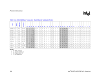
Page 181 highlights
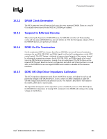
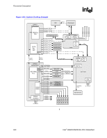
Functional Description R 10.3.2 10.3.3 10.3.4 10.3.5 DRAM Clock Generation The MCH generates three differential clock pairs for every supported DIMM. There are a total of 6 clock pairs driven directly by the MCH to 2 DIMMs per channel. Suspend to RAM and Resume When entering the Suspend-to-RAM (STR) state, the SDRAM controller will flush pending cycles and then enter all SDRAM rows into self refresh. In STR, the CKE signals remain LOW so the SDRAM devices will perform self-refresh. DDR2 On-Die Termination On-die termination (ODT) is a feature that allows a DRAM to turn on/off internal termination resistance for each DQ, DM, DQS, and DQS# signal for x8 and x16 configurations via the ODT control signals. The ODT feature is designed to improve signal integrity of the memory channel by allowing the termination resistance for the DQ, DM, DQS, and DQS# signals to be located inside the DRAM devices themselves, instead of on the motherboard. The MCH drives out the required ODT signals, based on memory configuration and which rank is being written to or read from, to the DRAM devices on a targeted DIMM rank to enable or disable their termination resistance. DDR2 Off-Chip Driver Impedance Calibration The OCD impedance adjustment mode allows the MCH to measure and adjust the pull-up and pull-down strength of the DRAM devices. It uses a series of EMRS commands to guide the DRAM through measurement and calibration cycles. This feature is described in more detail in the JEDEC DDR2 device specification. The algorithm and sequence of the adjustment cycles is handled by software. The MCH adjusts the DRAM driver impedance by issuing OCD commands to the DIMM and looking at the analog voltage on the DQ lines. Intel® 82925X/82925XE MCH Datasheet 181
-
 1
1 -
2
-
3
-
4
-
5
-
6
-
7
-
8
-
9
-
10
-
11
-
12
-
13
-
14
-
15
-
16
-
17
-
18
-
19
-
20
-
21
-
22
-
23
-
24
-
25
-
26
-
27
-
28
-
29
-
30
-
31
-
32
-
33
-
34
-
35
-
36
-
37
-
38
-
39
-
40
-
41
-
42
-
43
-
44
-
45
-
46
-
47
-
48
-
49
-
50
-
51
-
52
-
53
-
54
-
55
-
56
-
57
-
58
-
59
-
60
-
61
-
62
-
63
-
64
-
65
-
66
-
67
-
68
-
69
-
70
-
71
-
72
-
73
-
74
-
75
-
76
-
77
-
78
-
79
-
80
-
81
-
82
-
83
-
84
-
85
-
86
-
87
-
88
-
89
-
90
-
91
-
92
-
93
-
94
-
95
-
96
-
97
-
98
-
99
-
100
-
101
-
102
-
103
-
104
-
105
-
106
-
107
-
108
-
109
-
110
-
111
-
112
-
113
-
114
-
115
-
116
-
117
-
118
-
119
-
120
-
121
-
122
-
123
-
124
-
125
-
126
-
127
-
128
-
129
-
130
-
131
-
132
-
133
-
134
-
135
-
136
-
137
-
138
-
139
-
140
-
141
-
142
-
143
-
144
-
145
-
146
-
147
-
148
-
149
-
150
-
151
-
152
-
153
-
154
-
155
-
156
-
157
-
158
-
159
-
160
-
161
-
162
-
163
-
164
-
165
-
166
-
167
-
168
-
169
-
170
-
171
-
172
-
173
-
174
-
175
-
 176
176 -
 177
177 -
 178
178 -
 179
179 -
 180
180 -
 181
181 -
 182
182 -
 183
183 -
 184
184 -
 185
185 -
 186
186 -
187
-
188
-
189
-
190
-
191
-
192
-
193
-
194
-
195
-
196
-
197
-
198
-
199
-
200
-
201
-
202
-
203
-
204
-
205
-
206
-
207
-
208
-
209
-
210
-
211
-
212
-
213
-
214
-
215
-
216
-
217
-
218
-
219
-
220
-
221
-
222
-
223
-
224
-
225
-
226
-
227
-
228
-
229
-
230
-
231
-
232
-
233
-
234
-
235
-
236
-
237
-
238
-
239
-
240
-
241
-
242
 |
 |