Intel 925 Data Sheet - Page 191
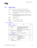
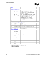
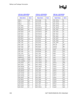
Symbol, Signal, Group, Parameter, Notes
 |
UPC - 683728067724
View all Intel 925 manuals
Add to My Manuals
Save this manual to your list of manuals |
Page 191 highlights
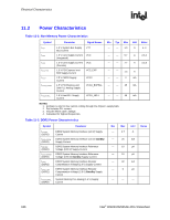
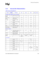
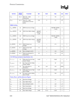
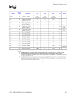
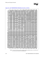
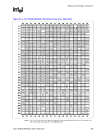
Electrical Characteristics R Symbol VCROSS VOL VOH IOL IOH VIL VIH ILEAK CIN VIL VIH ILEAK CIN Signal Group Parameter Min Nom Max Unit Notes3 (o) Crossing Voltage (p) Output Low Voltage (CMOS Outputs) (p) Output High Voltage (CMOS Outputs) (p) Output Low Current (CMOS Outputs) (p) Output High Current (CMOS Outputs) (p) Input Low Voltage (p) Input High Voltage (p) Crossing Voltage (p) Input Capacitance (n1) Input Low Voltage (n1) Input High Voltage (n1) Crossing Voltage (n1) Input Capacitance 0.45 x (VIH - VIL) - 2.1 - -1 - 1.4 - 3.0 - 2.0 - 4.690 0.5 x (VIH - VIL) - - - - - - - - - - - 0.55 x (VIH - VIL) 0.4 - 1 - 1.1 ±10 6.0 0.8 - ±100 5.370 V V V mA @VOL_HI max mA @VOH_HI min V V µA pF V V µA 0 < Vin < VCC3_3 pF NOTES: 1. Determined with 2x MCH DDR2 Buffer Strength Settings into a 50 Ω to 0.5xVCCSM (DDR2) test load. 2. Specified at the measurement point into a timing and voltage compliance test load as shown in Transmitter compliance eye diagram of the PCI Express Interface Specification 1.0a and measured over any 250 consecutive TX Uls. 3. Specified at the measurement point and measured over any 250 consecutive Uls. The test load shown in Receiver compliance eye diagram of the PCI Express Interface Specification 1.0a should be used as the RX device when taking measurements. § Intel® 82925X/82925XE MCH Datasheet 191
-
 1
1 -
2
-
3
-
4
-
5
-
6
-
7
-
8
-
9
-
10
-
11
-
12
-
13
-
14
-
15
-
16
-
17
-
18
-
19
-
20
-
21
-
22
-
23
-
24
-
25
-
26
-
27
-
28
-
29
-
30
-
31
-
32
-
33
-
34
-
35
-
36
-
37
-
38
-
39
-
40
-
41
-
42
-
43
-
44
-
45
-
46
-
47
-
48
-
49
-
50
-
51
-
52
-
53
-
54
-
55
-
56
-
57
-
58
-
59
-
60
-
61
-
62
-
63
-
64
-
65
-
66
-
67
-
68
-
69
-
70
-
71
-
72
-
73
-
74
-
75
-
76
-
77
-
78
-
79
-
80
-
81
-
82
-
83
-
84
-
85
-
86
-
87
-
88
-
89
-
90
-
91
-
92
-
93
-
94
-
95
-
96
-
97
-
98
-
99
-
100
-
101
-
102
-
103
-
104
-
105
-
106
-
107
-
108
-
109
-
110
-
111
-
112
-
113
-
114
-
115
-
116
-
117
-
118
-
119
-
120
-
121
-
122
-
123
-
124
-
125
-
126
-
127
-
128
-
129
-
130
-
131
-
132
-
133
-
134
-
135
-
136
-
137
-
138
-
139
-
140
-
141
-
142
-
143
-
144
-
145
-
146
-
147
-
148
-
149
-
150
-
151
-
152
-
153
-
154
-
155
-
156
-
157
-
158
-
159
-
160
-
161
-
162
-
163
-
164
-
165
-
166
-
167
-
168
-
169
-
170
-
171
-
172
-
173
-
174
-
175
-
176
-
177
-
178
-
179
-
180
-
181
-
182
-
183
-
184
-
185
-
 186
186 -
 187
187 -
 188
188 -
 189
189 -
 190
190 -
 191
191 -
 192
192 -
 193
193 -
 194
194 -
 195
195 -
 196
196 -
197
-
198
-
199
-
200
-
201
-
202
-
203
-
204
-
205
-
206
-
207
-
208
-
209
-
210
-
211
-
212
-
213
-
214
-
215
-
216
-
217
-
218
-
219
-
220
-
221
-
222
-
223
-
224
-
225
-
226
-
227
-
228
-
229
-
230
-
231
-
232
-
233
-
234
-
235
-
236
-
237
-
238
-
239
-
240
-
241
-
242
 |
 |