Intel 925 Data Sheet - Page 20
MCH Clocking, Power Management
 |
UPC - 683728067724
View all Intel 925 manuals
Add to My Manuals
Save this manual to your list of manuals |
Page 20 highlights
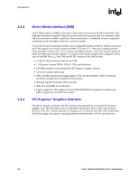
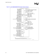
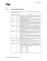
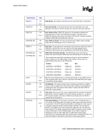
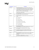
Introduction R 1.3.6 1.3.7 MCH Clocking The differential FSB clock (HCLKP/HCLKN) is set to 200 MHz on the 82925X MCH and 266 MHz on the 82925XE MCH. This supports FSB transfer rates of 800 MT/s for the 82925X MCH and FSB transfer rates of 1066 MT/s for the 82925XE MCH. The Host PLL generates 2X, 4X, and 8X versions of the host clock for internal optimizations. The MCH core clock is synchronized to the host clock. The internal and external memory clocks of 133 MHz, 200 MHz, and 266 MHz are generated from one of two MCH PLLs that use the host clock as a reference. This includes 2X and 4X for internal optimizations. The PCI Express core clock of 250 MHz is generated from a separate PCI Express PLL. This clock uses the fixed 100 MHz Serial Reference Clock (GCLKP/GCLKN) for reference. All of the above mentioned clocks are capable of tolerating Spread Spectrum clocking as defined in the Clock Generator specification. Host, Memory, and PCI Express* x16 Graphics PLLs, and all associated internal clocks are disabled until PWROK is asserted. Power Management MCH Power Management support includes: • PC99 suspend to DRAM support ("STR", mapped to ACPI state S3) • SMRAM space remapping to A0000h (128 KB) • Supports extended SMRAM space above 256 MB, additional 1-MB TSEG from the Base of graphics stolen memory (BSM) when enabled, and cacheable (cacheability controlled by processor) • ACPI Rev 1.0 compatible power management • Supports processor states: C0, C1, C2, C3, and C4 • Supports System states: S0, S1, S3, S4, and S5 • Supports processor Thermal Management 2 (TM2) • Microsoft Windows NT* Hardware Design Guide v1.0 compliant § 20 Intel® 82925X/82925XE MCH Datasheet
-
 1
1 -
2
-
3
-
4
-
5
-
6
-
7
-
8
-
9
-
10
-
11
-
12
-
13
-
14
-
 15
15 -
 16
16 -
 17
17 -
 18
18 -
 19
19 -
 20
20 -
 21
21 -
 22
22 -
 23
23 -
 24
24 -
 25
25 -
26
-
27
-
28
-
29
-
30
-
31
-
32
-
33
-
34
-
35
-
36
-
37
-
38
-
39
-
40
-
41
-
42
-
43
-
44
-
45
-
46
-
47
-
48
-
49
-
50
-
51
-
52
-
53
-
54
-
55
-
56
-
57
-
58
-
59
-
60
-
61
-
62
-
63
-
64
-
65
-
66
-
67
-
68
-
69
-
70
-
71
-
72
-
73
-
74
-
75
-
76
-
77
-
78
-
79
-
80
-
81
-
82
-
83
-
84
-
85
-
86
-
87
-
88
-
89
-
90
-
91
-
92
-
93
-
94
-
95
-
96
-
97
-
98
-
99
-
100
-
101
-
102
-
103
-
104
-
105
-
106
-
107
-
108
-
109
-
110
-
111
-
112
-
113
-
114
-
115
-
116
-
117
-
118
-
119
-
120
-
121
-
122
-
123
-
124
-
125
-
126
-
127
-
128
-
129
-
130
-
131
-
132
-
133
-
134
-
135
-
136
-
137
-
138
-
139
-
140
-
141
-
142
-
143
-
144
-
145
-
146
-
147
-
148
-
149
-
150
-
151
-
152
-
153
-
154
-
155
-
156
-
157
-
158
-
159
-
160
-
161
-
162
-
163
-
164
-
165
-
166
-
167
-
168
-
169
-
170
-
171
-
172
-
173
-
174
-
175
-
176
-
177
-
178
-
179
-
180
-
181
-
182
-
183
-
184
-
185
-
186
-
187
-
188
-
189
-
190
-
191
-
192
-
193
-
194
-
195
-
196
-
197
-
198
-
199
-
200
-
201
-
202
-
203
-
204
-
205
-
206
-
207
-
208
-
209
-
210
-
211
-
212
-
213
-
214
-
215
-
216
-
217
-
218
-
219
-
220
-
221
-
222
-
223
-
224
-
225
-
226
-
227
-
228
-
229
-
230
-
231
-
232
-
233
-
234
-
235
-
236
-
237
-
238
-
239
-
240
-
241
-
242
 |
 |