Intel 925 Data Sheet - Page 28
DDR2 DRAM Reference and Compensation, PCI Express* x16 Graphics Port Signals - graphic drivers
 |
UPC - 683728067724
View all Intel 925 manuals
Add to My Manuals
Save this manual to your list of manuals |
Page 28 highlights
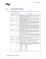
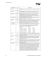
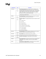
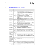
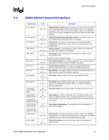
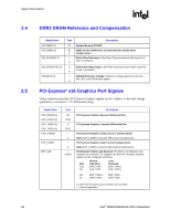
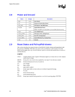
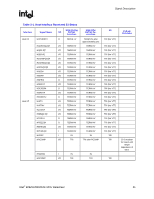
Signal Description R 2.4 DDR2 DRAM Reference and Compensation 2.5 Signal Name SRCOMP[1:0] SOCOMP[1:0] SM_SLEWIN[1:0] SM_SLEWOUT[1:0] SMVREF[1:0] Type Description I/O System Memory RCOMP I/O DDR2 On-Die DRAM Over Current Detection (OCD) driver A compensation I Buffer Slew Rate Input: Slew Rate Characterization buffer input for X and Y orientation. A O Buffer Slew Rate Output: Slew Rate Characterization buffer output for X and Y orientation A I SDRAM Reference Voltage: Reference voltage inputs for each DQ, DM, DQS, and DQS# input signals. A PCI Express* x16 Graphics Port Signals Unless otherwise specified, PCI Express Graphics signals are AC coupled, so the only voltage specified is a maximum 1.2 V differential swing. Signal Name EXP_RXN[15:0] EXP_RXP[15:0] EXP_TXN[15:0] EXP_TXP[15:0] EXP_COMPO EXP_COMPI EXP_SLR Type I/O PCIE O PCIE I A I A I CMOS Description PCI Express Graphics Receive Differential Pair PCI Express Graphics Transmit Differential Pair PCI Express Graphics Output Current Compensation Note: EXP_COMP0 is used for DMI current compensation. PCI Express Graphics Input Current Compensation Note: EXP_COMPI is used for DMI current compensation. PCI Express* Static Lane Reversal: The MCH's PCI Express lane numbers are reversed. For example, the MCH PCI Express interface signals can be configured as follows: Normal Lane Ball Operation Reversed C10 EXP_TXP0 EXP_TXP15 A9 EXP_TXP1 EXP_TXP14 ... ... ... N3 EXP_TXP14... EXP_TXP1... P1 EXP_TXP15 EXP_TXP0 0 = MCH's PCI Express lane numbers are reversed 1 = Normal operation 28 Intel® 82925X/82925XE MCH Datasheet
-
 1
1 -
2
-
3
-
4
-
5
-
6
-
7
-
8
-
9
-
10
-
11
-
12
-
13
-
14
-
15
-
16
-
17
-
18
-
19
-
20
-
21
-
22
-
 23
23 -
 24
24 -
 25
25 -
 26
26 -
 27
27 -
 28
28 -
 29
29 -
 30
30 -
 31
31 -
 32
32 -
 33
33 -
34
-
35
-
36
-
37
-
38
-
39
-
40
-
41
-
42
-
43
-
44
-
45
-
46
-
47
-
48
-
49
-
50
-
51
-
52
-
53
-
54
-
55
-
56
-
57
-
58
-
59
-
60
-
61
-
62
-
63
-
64
-
65
-
66
-
67
-
68
-
69
-
70
-
71
-
72
-
73
-
74
-
75
-
76
-
77
-
78
-
79
-
80
-
81
-
82
-
83
-
84
-
85
-
86
-
87
-
88
-
89
-
90
-
91
-
92
-
93
-
94
-
95
-
96
-
97
-
98
-
99
-
100
-
101
-
102
-
103
-
104
-
105
-
106
-
107
-
108
-
109
-
110
-
111
-
112
-
113
-
114
-
115
-
116
-
117
-
118
-
119
-
120
-
121
-
122
-
123
-
124
-
125
-
126
-
127
-
128
-
129
-
130
-
131
-
132
-
133
-
134
-
135
-
136
-
137
-
138
-
139
-
140
-
141
-
142
-
143
-
144
-
145
-
146
-
147
-
148
-
149
-
150
-
151
-
152
-
153
-
154
-
155
-
156
-
157
-
158
-
159
-
160
-
161
-
162
-
163
-
164
-
165
-
166
-
167
-
168
-
169
-
170
-
171
-
172
-
173
-
174
-
175
-
176
-
177
-
178
-
179
-
180
-
181
-
182
-
183
-
184
-
185
-
186
-
187
-
188
-
189
-
190
-
191
-
192
-
193
-
194
-
195
-
196
-
197
-
198
-
199
-
200
-
201
-
202
-
203
-
204
-
205
-
206
-
207
-
208
-
209
-
210
-
211
-
212
-
213
-
214
-
215
-
216
-
217
-
218
-
219
-
220
-
221
-
222
-
223
-
224
-
225
-
226
-
227
-
228
-
229
-
230
-
231
-
232
-
233
-
234
-
235
-
236
-
237
-
238
-
239
-
240
-
241
-
242
 |
 |