Intel 925 Data Sheet - Page 35
Register Description, Register Terminology
 |
UPC - 683728067724
View all Intel 925 manuals
Add to My Manuals
Save this manual to your list of manuals |
Page 35 highlights
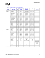
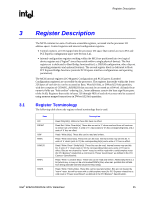
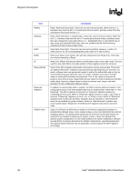
Register Description R 3 3.1 Register Description The MCH contains two sets of software accessible registers, accessed via the processor I/O address space: Control registers and internal configuration registers. • Control registers are I/O mapped into the processor I/O space that control access to PCI and PCI Express configuration space (see Section 3.4). • Internal configuration registers residing within the MCH are partitioned into two logical device register sets ("logical" since they reside within a single physical device). The first register set is dedicated to Host Bridge functionality (i.e. DRAM configuration, other chip-set operating parameters and optional features). The second register block is dedicated to HostPCI Express Bridge functions (controls PCI Express interface configurations and operating parameters). The MCH internal registers (I/O Mapped, Configuration and PCI Express Extended Configuration registers) are accessible by the processor. The registers that reside within the lower 256 bytes of each device can be accessed as Byte, Word (16-bit), or DWord (32-bit) quantities, with the exception of CONFIG_ADDRESS that can only be accessed as a DWord. All multi-byte numeric fields use "little-endian" ordering (i.e., lower addresses contain the least significant parts of the field). Registers that reside in bytes 256 through 4095 of each device may only be accessed using memory mapped transactions in DWord (32-bit) quantities. Register Terminology The following table shows the register-related terminology that is used. Item RO RS/WC R/W R/WC R/WC/S R/W/L R/W/S Description Read Only bit(s). Writes to these bits have no effect. Read Set / Write Clear bit(s). These bits are set to '1' when read and then will continue to remain set until written. A write of '1' clears (sets to '0') the corresponding bit(s) and a write of '0' has no effect. Read / Write bit(s). These bits can be read and written. Read / Write Clear bit(s). These bits can be read. Internal events may set this bit. A write of '1' clears (sets to '0') the corresponding bit(s) and a write of '0' has no effect. Read / Write Clear / Sticky bit(s). These bits can be read. Internal events may set this bit. A write of '1' clears (sets to '0') the corresponding bit(s) and a write of '0' has no effect. Bits are not cleared by "warm" reset, but will be reset with a cold/complete reset (for PCI Express* related bits a cold reset is "Power Good Reset" as defined in the PCI Express* Specification). Read / Write / Lockable bit(s). These bits can be read and written. Additionally there is a bit (which may or may not be a bit marked R/W/L) that, when set, prohibits this bit field from being writeable (bit field becomes Read Only). Read / Write / Sticky bit(s). These bits can be read and written. Bits are not cleared by "warm" reset, but will be reset with a cold/complete reset (for PCI Express related bits a cold reset is "Power Good Reset" as defined in the PCI Express* Specification). Intel® 82925X/82925XE MCH Datasheet 35
-
 1
1 -
2
-
3
-
4
-
5
-
6
-
7
-
8
-
9
-
10
-
11
-
12
-
13
-
14
-
15
-
16
-
17
-
18
-
19
-
20
-
21
-
22
-
23
-
24
-
25
-
26
-
27
-
28
-
29
-
 30
30 -
 31
31 -
 32
32 -
 33
33 -
 34
34 -
 35
35 -
 36
36 -
 37
37 -
 38
38 -
 39
39 -
 40
40 -
41
-
42
-
43
-
44
-
45
-
46
-
47
-
48
-
49
-
50
-
51
-
52
-
53
-
54
-
55
-
56
-
57
-
58
-
59
-
60
-
61
-
62
-
63
-
64
-
65
-
66
-
67
-
68
-
69
-
70
-
71
-
72
-
73
-
74
-
75
-
76
-
77
-
78
-
79
-
80
-
81
-
82
-
83
-
84
-
85
-
86
-
87
-
88
-
89
-
90
-
91
-
92
-
93
-
94
-
95
-
96
-
97
-
98
-
99
-
100
-
101
-
102
-
103
-
104
-
105
-
106
-
107
-
108
-
109
-
110
-
111
-
112
-
113
-
114
-
115
-
116
-
117
-
118
-
119
-
120
-
121
-
122
-
123
-
124
-
125
-
126
-
127
-
128
-
129
-
130
-
131
-
132
-
133
-
134
-
135
-
136
-
137
-
138
-
139
-
140
-
141
-
142
-
143
-
144
-
145
-
146
-
147
-
148
-
149
-
150
-
151
-
152
-
153
-
154
-
155
-
156
-
157
-
158
-
159
-
160
-
161
-
162
-
163
-
164
-
165
-
166
-
167
-
168
-
169
-
170
-
171
-
172
-
173
-
174
-
175
-
176
-
177
-
178
-
179
-
180
-
181
-
182
-
183
-
184
-
185
-
186
-
187
-
188
-
189
-
190
-
191
-
192
-
193
-
194
-
195
-
196
-
197
-
198
-
199
-
200
-
201
-
202
-
203
-
204
-
205
-
206
-
207
-
208
-
209
-
210
-
211
-
212
-
213
-
214
-
215
-
216
-
217
-
218
-
219
-
220
-
221
-
222
-
223
-
224
-
225
-
226
-
227
-
228
-
229
-
230
-
231
-
232
-
233
-
234
-
235
-
236
-
237
-
238
-
239
-
240
-
241
-
242
 |
 |