Intel 925 Data Sheet - Page 38
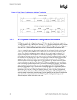
General Routing Configuration Accesses, Standard PCI Bus Configuration Mechanism
 |
UPC - 683728067724
View all Intel 925 manuals
Add to My Manuals
Save this manual to your list of manuals |
Page 38 highlights
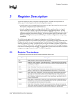
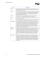
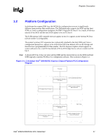
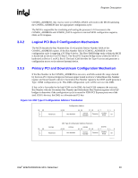
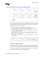
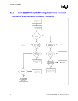
Register Description R The MCH contains the following PCI devices within a single physical component. The configuration registers for the devices are mapped as devices residing on PCI bus 0. • Device 0 - Host Bridge/DRAM Controller: Logically this appears as a PCI device residing on PCI bus 0. Device 0 contains the standard PCI header registers, PCI Express base address register, DRAM control (including thermal/throttling control), and configuration for the DMI and other MCH specific registers. • Device 1- Host-PCI Express Bridge. Logically this appears as a "virtual" PCI-to-PCI bridge residing on PCI bus 0 and is compliant with PCI Express* Specification Revision 1.0a. Device 1 contains the standard PCI-to-PCI bridge registers and the standard PCI Express/PCI configuration registers (including the PCI Express memory address mapping). It also contains Isochronous and Virtual Channel controls in the PCI Express extended configuration space. Table 3-1. Device Number Assignment for Internal MCH Devices MCH Function Host Bridge / DRAM Controller Host-to-PCI Express* Bridge (virtual P2P) Device# Device 0 Device 1 3.3 3.3.1 General Routing Configuration Accesses The MCH supports two PCI related interfaces: DMI and PCI Express. PCI and PCI Express configuration cycles are selectively routed to one of these interfaces. The MCH is responsible for routing configuration cycles to the proper interface. Configuration cycles to the Intel ICH6 internal devices and Primary PCI (including downstream devices) are routed to the Intel ICH6 via DMI. Configuration cycles to both the PCI Express Graphics PCI compatibility configuration space and the PCI Express Graphics extended configuration space are routed to the PCI Express Graphics port. A detailed description of the mechanism for translating processor I/O bus cycles to configuration cycles is described below. Standard PCI Bus Configuration Mechanism The PCI Bus defines a slot based "configuration space" that allows each device to contain up to 8 functions with each function containing up to 256 8-bit configuration registers. The PCI specification defines two bus cycles to access the PCI configuration space: Configuration Read and Configuration Write. Memory and I/O spaces are supported directly by the processor. Configuration space is supported by a mapping mechanism implemented within the MCH. The configuration access mechanism makes use of the CONFIG_ADDRESS Register (at I/O address 0CF8h though 0CFBh) and CONFIG_DATA Register (at I/O address 0CFCh though 0CFFh). To reference a configuration register a DW I/O write cycle is used to place a value into CONFIG_ADDRESS that specifies the PCI bus, the device on that bus, the function within the device, and a specific configuration register of the device function being accessed. CONFIG_ADDRESS [31] must be 1 to enable a configuration cycle. CONFIG_DATA then becomes a window into the four bytes of configuration space specified by the contents of 38 Intel® 82925X/82925XE MCH Datasheet
-
 1
1 -
2
-
3
-
4
-
5
-
6
-
7
-
8
-
9
-
10
-
11
-
12
-
13
-
14
-
15
-
16
-
17
-
18
-
19
-
20
-
21
-
22
-
23
-
24
-
25
-
26
-
27
-
28
-
29
-
30
-
31
-
32
-
 33
33 -
 34
34 -
 35
35 -
 36
36 -
 37
37 -
 38
38 -
 39
39 -
 40
40 -
 41
41 -
 42
42 -
 43
43 -
44
-
45
-
46
-
47
-
48
-
49
-
50
-
51
-
52
-
53
-
54
-
55
-
56
-
57
-
58
-
59
-
60
-
61
-
62
-
63
-
64
-
65
-
66
-
67
-
68
-
69
-
70
-
71
-
72
-
73
-
74
-
75
-
76
-
77
-
78
-
79
-
80
-
81
-
82
-
83
-
84
-
85
-
86
-
87
-
88
-
89
-
90
-
91
-
92
-
93
-
94
-
95
-
96
-
97
-
98
-
99
-
100
-
101
-
102
-
103
-
104
-
105
-
106
-
107
-
108
-
109
-
110
-
111
-
112
-
113
-
114
-
115
-
116
-
117
-
118
-
119
-
120
-
121
-
122
-
123
-
124
-
125
-
126
-
127
-
128
-
129
-
130
-
131
-
132
-
133
-
134
-
135
-
136
-
137
-
138
-
139
-
140
-
141
-
142
-
143
-
144
-
145
-
146
-
147
-
148
-
149
-
150
-
151
-
152
-
153
-
154
-
155
-
156
-
157
-
158
-
159
-
160
-
161
-
162
-
163
-
164
-
165
-
166
-
167
-
168
-
169
-
170
-
171
-
172
-
173
-
174
-
175
-
176
-
177
-
178
-
179
-
180
-
181
-
182
-
183
-
184
-
185
-
186
-
187
-
188
-
189
-
190
-
191
-
192
-
193
-
194
-
195
-
196
-
197
-
198
-
199
-
200
-
201
-
202
-
203
-
204
-
205
-
206
-
207
-
208
-
209
-
210
-
211
-
212
-
213
-
214
-
215
-
216
-
217
-
218
-
219
-
220
-
221
-
222
-
223
-
224
-
225
-
226
-
227
-
228
-
229
-
230
-
231
-
232
-
233
-
234
-
235
-
236
-
237
-
238
-
239
-
240
-
241
-
242
 |
 |