Intel 925 Data Sheet - Page 39
Logical PCI Bus 0 Configuration Mechanism, Primary PCI and Downstream Configuration Mechanism
 |
UPC - 683728067724
View all Intel 925 manuals
Add to My Manuals
Save this manual to your list of manuals |
Page 39 highlights
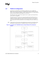
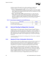
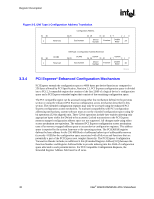
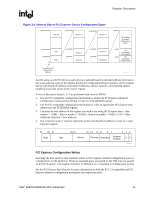
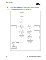
Register Description R CONFIG_ADDRESS. Any read or write to CONFIG_DATA will result in the MCH translating the CONFIG_ADDRESS into the appropriate configuration cycle. The MCH is responsible for translating and routing the processor's I/O accesses to the CONFIG_ADDRESS and CONFIG_DATA registers to internal MCH configuration registers, DMI, or PCI Express. 3.3.2 Logical PCI Bus 0 Configuration Mechanism The MCH decodes the Bus Number (bits 23:16) and the Device Number fields of the CONFIG_ADDRESS register. If the Bus Number field of CONFIG_ADDRESS is 0 the configuration cycle is targeting a PCI Bus 0 device. The Host-DMI Bridge entity within the MCH is hardwired as Device 0 on PCI Bus 0. The Host-PCI Express Bridge entity within the MCH is hardwired as Device 1 on PCI Bus 0. The Intel ICH6 decodes the Type 0 access and generates a configuration access to the selected internal device. 3.3.3 Primary PCI and Downstream Configuration Mechanism If the Bus Number in the CONFIG_ADDRESS is non-zero, and falls outside the range claimed by the Host-PCI Express bridge (not between upper bound in device's Subordinate Bus Number register and lower bound in device's Secondary Bus Number register), the MCH would generate a Type 1 DMI configuration cycle. This DMI configuration cycle will be sent over the DMI. If the cycle is forwarded to the Intel ICH6 via the DMI, the Intel ICH6 compares the non-zero Bus Number with the Secondary Bus Number and Subordinate Bus Number registers of its P2P bridges to determine if the configuration cycle is meant for ICH6 PCI Express ports one of the Intel ICH6's devices, the DMI, or a downstream PCI bus. Figure 3-2. DMI Type 0 Configuration Address Translation 31 30 1 Reserved Configuration Address 24 23 Bus Number 16 15 11 10 87 21 0 Device Number Function Double Word XX 31 30 1 OCFBh Reserved DMI Type 0 Configuration Address Extension 24 23 OCFAh Bus Number OCF9h 16 15 11 10 OCF8h 87 21 0 Device Number Function Double Word 00 DMI_Typ0_Config Intel® 82925X/82925XE MCH Datasheet 39
-
 1
1 -
2
-
3
-
4
-
5
-
6
-
7
-
8
-
9
-
10
-
11
-
12
-
13
-
14
-
15
-
16
-
17
-
18
-
19
-
20
-
21
-
22
-
23
-
24
-
25
-
26
-
27
-
28
-
29
-
30
-
31
-
32
-
33
-
 34
34 -
 35
35 -
 36
36 -
 37
37 -
 38
38 -
 39
39 -
 40
40 -
 41
41 -
 42
42 -
 43
43 -
 44
44 -
45
-
46
-
47
-
48
-
49
-
50
-
51
-
52
-
53
-
54
-
55
-
56
-
57
-
58
-
59
-
60
-
61
-
62
-
63
-
64
-
65
-
66
-
67
-
68
-
69
-
70
-
71
-
72
-
73
-
74
-
75
-
76
-
77
-
78
-
79
-
80
-
81
-
82
-
83
-
84
-
85
-
86
-
87
-
88
-
89
-
90
-
91
-
92
-
93
-
94
-
95
-
96
-
97
-
98
-
99
-
100
-
101
-
102
-
103
-
104
-
105
-
106
-
107
-
108
-
109
-
110
-
111
-
112
-
113
-
114
-
115
-
116
-
117
-
118
-
119
-
120
-
121
-
122
-
123
-
124
-
125
-
126
-
127
-
128
-
129
-
130
-
131
-
132
-
133
-
134
-
135
-
136
-
137
-
138
-
139
-
140
-
141
-
142
-
143
-
144
-
145
-
146
-
147
-
148
-
149
-
150
-
151
-
152
-
153
-
154
-
155
-
156
-
157
-
158
-
159
-
160
-
161
-
162
-
163
-
164
-
165
-
166
-
167
-
168
-
169
-
170
-
171
-
172
-
173
-
174
-
175
-
176
-
177
-
178
-
179
-
180
-
181
-
182
-
183
-
184
-
185
-
186
-
187
-
188
-
189
-
190
-
191
-
192
-
193
-
194
-
195
-
196
-
197
-
198
-
199
-
200
-
201
-
202
-
203
-
204
-
205
-
206
-
207
-
208
-
209
-
210
-
211
-
212
-
213
-
214
-
215
-
216
-
217
-
218
-
219
-
220
-
221
-
222
-
223
-
224
-
225
-
226
-
227
-
228
-
229
-
230
-
231
-
232
-
233
-
234
-
235
-
236
-
237
-
238
-
239
-
240
-
241
-
242
 |
 |