Intel 925 Data Sheet - Page 41
PCI Express Configuration Writes
 |
UPC - 683728067724
View all Intel 925 manuals
Add to My Manuals
Save this manual to your list of manuals |
Page 41 highlights
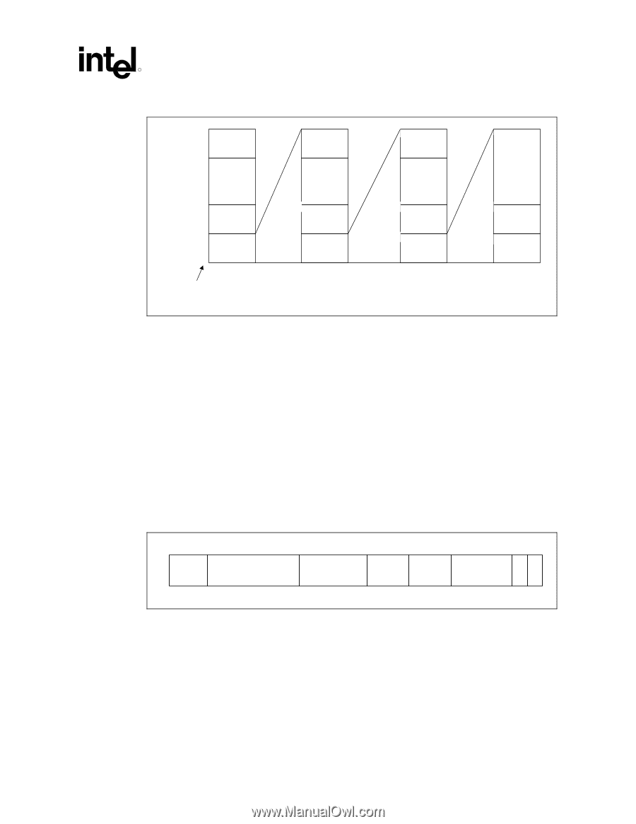
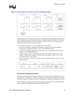
Register Description R Figure 3-4. Memory Map to PCI Express* Device Configuration Space 0xFFFFFFFh Bus 255 0xFFFFFh Device 31 0xFFFFFh Function 7 0x1FFFFFh 0xFFFFFh 0h Bus 1 Bus 0 Located By PCI Express Base Address 0xFFFFh 0x7FFFh Device 1 Device 0 0xFFFFh Function 1 0x7FFFh Function 0 0xFFFh PCI Express Extended Configuration Space 0xFFh PCI Compatible Config Space 0x3Fh PCI Compatible Config Header MemMap_PCIExpress Just the same as with PCI devices, each device is selected based on decoded address information that is provided as a part of the address portion of Configuration Request packets. A PCI Express device will decode all address information fields (bus, device, function, and extended address numbers) to provide access to the correct register. To access this space (steps 1, 2, 3 are performed only once by BIOS) 1. Use the PCI compatible configuration mechanism to enable the PCI Express enhanced configuration mechanism by writing 1 to bit 31 of the DEVEN register. 2. Use the PCI compatible configuration mechanism to write an appropriate PCI Express base address into the PCIEXBAR register. 3. Calculate the host address of the register you wish to set using (PCI Express base + (bus number * 1 MB) + (device number * 32 KB) + (function number * 4 KB) + (1 B * offset within the function) = host address). 4. Use a memory write or memory read cycle to the calculated host address to write to or read from that register. 31 28 27 Base Bus 20 19 15 14 12 11 8 7 210 Device Function Extended Register Number XX Config_Write PCI Express Configuration Writes Internally the host interface unit translates writes to PCI Express extended configuration space to configurations on the backbone. Writes to extended space are posted on the FSB, but non-posted on the PCI Express* x16 Graphics Interface or DMI pins (i.e., translated to configuration writes). See the PCI Express Specification for more information on both the PCI 2.3 compatible and PCI Express enhanced configuration mechanism and transaction rules. Intel® 82925X/82925XE MCH Datasheet 41
-
 1
1 -
2
-
3
-
4
-
5
-
6
-
7
-
8
-
9
-
10
-
11
-
12
-
13
-
14
-
15
-
16
-
17
-
18
-
19
-
20
-
21
-
22
-
23
-
24
-
25
-
26
-
27
-
28
-
29
-
30
-
31
-
32
-
33
-
34
-
35
-
 36
36 -
 37
37 -
 38
38 -
 39
39 -
 40
40 -
 41
41 -
 42
42 -
 43
43 -
 44
44 -
 45
45 -
 46
46 -
47
-
48
-
49
-
50
-
51
-
52
-
53
-
54
-
55
-
56
-
57
-
58
-
59
-
60
-
61
-
62
-
63
-
64
-
65
-
66
-
67
-
68
-
69
-
70
-
71
-
72
-
73
-
74
-
75
-
76
-
77
-
78
-
79
-
80
-
81
-
82
-
83
-
84
-
85
-
86
-
87
-
88
-
89
-
90
-
91
-
92
-
93
-
94
-
95
-
96
-
97
-
98
-
99
-
100
-
101
-
102
-
103
-
104
-
105
-
106
-
107
-
108
-
109
-
110
-
111
-
112
-
113
-
114
-
115
-
116
-
117
-
118
-
119
-
120
-
121
-
122
-
123
-
124
-
125
-
126
-
127
-
128
-
129
-
130
-
131
-
132
-
133
-
134
-
135
-
136
-
137
-
138
-
139
-
140
-
141
-
142
-
143
-
144
-
145
-
146
-
147
-
148
-
149
-
150
-
151
-
152
-
153
-
154
-
155
-
156
-
157
-
158
-
159
-
160
-
161
-
162
-
163
-
164
-
165
-
166
-
167
-
168
-
169
-
170
-
171
-
172
-
173
-
174
-
175
-
176
-
177
-
178
-
179
-
180
-
181
-
182
-
183
-
184
-
185
-
186
-
187
-
188
-
189
-
190
-
191
-
192
-
193
-
194
-
195
-
196
-
197
-
198
-
199
-
200
-
201
-
202
-
203
-
204
-
205
-
206
-
207
-
208
-
209
-
210
-
211
-
212
-
213
-
214
-
215
-
216
-
217
-
218
-
219
-
220
-
221
-
222
-
223
-
224
-
225
-
226
-
227
-
228
-
229
-
230
-
231
-
232
-
233
-
234
-
235
-
236
-
237
-
238
-
239
-
240
-
241
-
242
 |
 |