Intel 925 Data Sheet - Page 45
Host Bridge/DRAM Controller Registers (D0:F0
 |
UPC - 683728067724
View all Intel 925 manuals
Add to My Manuals
Save this manual to your list of manuals |
Page 45 highlights
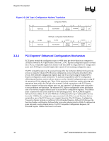
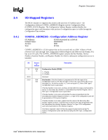
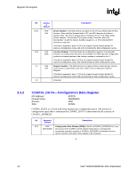
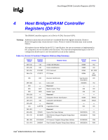
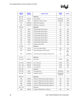
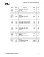
Host Bridge/DRAM Controller Registers (D0:F0) R 4 Host Bridge/DRAM Controller Registers (D0:F0) The DRAM Controller registers are in Device 0 (D0), Function 0 (F0). Warning: Address locations that are not listed are considered Reserved registers locations. Reads to Reserved registers may return non-zero values. Writes to reserved locations may cause system failures. All registers that are defined in the PCI 2.3 specification, but are not necessary or implemented in this component are not included in this document. The reserved/unimplemented space in the PCI configuration header space is not documented as such in this summary. Table 4-1. Device 0 Function 0 Register Address Map Summary Address Offset 00h-01h 02h-03h 04h-05h 06h-07h 08h 09h-0Bh 0Ch 0Dh 0Eh 0Fh-2Bh 2Ch-2Dh 2Eh-2Fh 30h-33h 34h 35h-3Fh 40h-43h 44h-47h 48h-4Bh 4Ch-4Fh Register Symbol VID DID PCICMD PCISTS Register Name Vendor Identification Device Identification PCI Command PCI Status RID Revision Identification CC - MLT HDR - SVID SID - CAPPTR - EPBAR MCHBAR PCIEXBAR DMIBAR Class Code Reserved Master Latency Timer Header Type Reserved Subsystem Vendor Identification Subsystem Identification Reserved Capabilities Pointer Reserved Egress Port Base Address MCH Memory Mapped Register Range Base Address PCI Express* Register Range Base Address Root Complex Register Range Base Address Default Value 8086h 2580h 0006h 0090h See Register Description 060000h - 00h 00h - 0000h 0000h - E0h - 00000000h 00000000h Access RO RO RO, R/W RO, R/W/C RO RO - RO RO - R/W/O R/W/O - RO - RO R/W E0000000h R/W 00000000h R/W Intel® 82925X/82925XE MCH Datasheet 45
-
 1
1 -
2
-
3
-
4
-
5
-
6
-
7
-
8
-
9
-
10
-
11
-
12
-
13
-
14
-
15
-
16
-
17
-
18
-
19
-
20
-
21
-
22
-
23
-
24
-
25
-
26
-
27
-
28
-
29
-
30
-
31
-
32
-
33
-
34
-
35
-
36
-
37
-
38
-
39
-
 40
40 -
 41
41 -
 42
42 -
 43
43 -
 44
44 -
 45
45 -
 46
46 -
 47
47 -
 48
48 -
 49
49 -
 50
50 -
51
-
52
-
53
-
54
-
55
-
56
-
57
-
58
-
59
-
60
-
61
-
62
-
63
-
64
-
65
-
66
-
67
-
68
-
69
-
70
-
71
-
72
-
73
-
74
-
75
-
76
-
77
-
78
-
79
-
80
-
81
-
82
-
83
-
84
-
85
-
86
-
87
-
88
-
89
-
90
-
91
-
92
-
93
-
94
-
95
-
96
-
97
-
98
-
99
-
100
-
101
-
102
-
103
-
104
-
105
-
106
-
107
-
108
-
109
-
110
-
111
-
112
-
113
-
114
-
115
-
116
-
117
-
118
-
119
-
120
-
121
-
122
-
123
-
124
-
125
-
126
-
127
-
128
-
129
-
130
-
131
-
132
-
133
-
134
-
135
-
136
-
137
-
138
-
139
-
140
-
141
-
142
-
143
-
144
-
145
-
146
-
147
-
148
-
149
-
150
-
151
-
152
-
153
-
154
-
155
-
156
-
157
-
158
-
159
-
160
-
161
-
162
-
163
-
164
-
165
-
166
-
167
-
168
-
169
-
170
-
171
-
172
-
173
-
174
-
175
-
176
-
177
-
178
-
179
-
180
-
181
-
182
-
183
-
184
-
185
-
186
-
187
-
188
-
189
-
190
-
191
-
192
-
193
-
194
-
195
-
196
-
197
-
198
-
199
-
200
-
201
-
202
-
203
-
204
-
205
-
206
-
207
-
208
-
209
-
210
-
211
-
212
-
213
-
214
-
215
-
216
-
217
-
218
-
219
-
220
-
221
-
222
-
223
-
224
-
225
-
226
-
227
-
228
-
229
-
230
-
231
-
232
-
233
-
234
-
235
-
236
-
237
-
238
-
239
-
240
-
241
-
242
 |
 |