Intel 925 Data Sheet - Page 50
PCISTS-PCI Status D0:F0, PCI Device, Address Offset, Default Value, Access, RO, R/W/C
 |
UPC - 683728067724
View all Intel 925 manuals
Add to My Manuals
Save this manual to your list of manuals |
Page 50 highlights
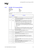
Host Bridge/DRAM Controller Registers (D0:F0) R 4.1.4 PCISTS-PCI Status (D0:F0) PCI Device: Address Offset: Default Value: Access: Size: 0 06h 0090h RO, R/W/C 16 bits This status register reports the occurrence of error events on Device 0's PCI interface. Since the MCH Device 0 does not physically reside on Primary PCI, many of the bits are not implemented. Bit Access & Default Description 15 RO Detected Parity Error (DPE): Hhardwired to a 0. 0b 14 R/W/C Signaled System Error (SSE): Software clears this bit by writing a 1 to it. 0b 1 = The MCH Device 0 generated an SERR message over DMI for any enabled Device 0 error condition. Device 0 error conditions are enabled in the PCICMD, and ERRCMD registers. Device 0 error flags are read/reset from the PCISTS, or ERRSTS registers. 13 R/WC Received Master Abort Status (RMAS): Software clears this bit by writing a 1 to 0b it. 1 = MCH generated a DMI request that receives an Unsupported Request completion packet. 12 R/WC Received Target Abort Status (RTAS): Software clears this bit by writing a 1 to 0b it. 1 = MCH generated a DMI request that receives a Completer Abort completion packet. 11 RO Signaled Target Abort Status (STAS): The MCH will not generate a Target 0b Abort DMI completion packet or Special Cycle. This bit is not implemented in the MCH and is hardwired to a 0. 10:9 RO DEVSEL Timing (DEVT): These bits are hardwired to "00". Device 0 does not 00b physically connect to Primary PCI. These bits are set to "00" (fast decode) so that optimum DEVSEL timing for Primary PCI is not limited by the MCH. 8 RO Master Data Parity Error Detected (DPD): PERR signaling and messaging are 0b not implemented by the MCH; therefore, this bit is hardwired to 0. 7 RO Fast Back-to-Back (FB2B): Hardwired to 1. Device 0 does not physically 1b connect to Primary PCI. This bit is set to 1 (indicating fast back-to-back capability) so that the optimum setting for Primary PCI is not limited by the MCH. 6 Reserved 5 RO 66 MHz Capable: Does not apply to PCI Express*. Hardwired to 0. 0b 4 RO Capability List (CLIST): This bit is hardwired to 1 to indicate to the configuration 1b software that this device/function implements a list of new capabilities. A list of new capabilities is accessed via register CAPPTR at configuration address offset 34h. Register CAPPTR contains an offset pointing to the start address within configuration space of this device where the Capability standard register resides. 3:0 Reserved 50 Intel® 82925X/82925XE MCH Datasheet
-
 1
1 -
2
-
3
-
4
-
5
-
6
-
7
-
8
-
9
-
10
-
11
-
12
-
13
-
14
-
15
-
16
-
17
-
18
-
19
-
20
-
21
-
22
-
23
-
24
-
25
-
26
-
27
-
28
-
29
-
30
-
31
-
32
-
33
-
34
-
35
-
36
-
37
-
38
-
39
-
40
-
41
-
42
-
43
-
44
-
 45
45 -
 46
46 -
 47
47 -
 48
48 -
 49
49 -
 50
50 -
 51
51 -
 52
52 -
 53
53 -
 54
54 -
 55
55 -
56
-
57
-
58
-
59
-
60
-
61
-
62
-
63
-
64
-
65
-
66
-
67
-
68
-
69
-
70
-
71
-
72
-
73
-
74
-
75
-
76
-
77
-
78
-
79
-
80
-
81
-
82
-
83
-
84
-
85
-
86
-
87
-
88
-
89
-
90
-
91
-
92
-
93
-
94
-
95
-
96
-
97
-
98
-
99
-
100
-
101
-
102
-
103
-
104
-
105
-
106
-
107
-
108
-
109
-
110
-
111
-
112
-
113
-
114
-
115
-
116
-
117
-
118
-
119
-
120
-
121
-
122
-
123
-
124
-
125
-
126
-
127
-
128
-
129
-
130
-
131
-
132
-
133
-
134
-
135
-
136
-
137
-
138
-
139
-
140
-
141
-
142
-
143
-
144
-
145
-
146
-
147
-
148
-
149
-
150
-
151
-
152
-
153
-
154
-
155
-
156
-
157
-
158
-
159
-
160
-
161
-
162
-
163
-
164
-
165
-
166
-
167
-
168
-
169
-
170
-
171
-
172
-
173
-
174
-
175
-
176
-
177
-
178
-
179
-
180
-
181
-
182
-
183
-
184
-
185
-
186
-
187
-
188
-
189
-
190
-
191
-
192
-
193
-
194
-
195
-
196
-
197
-
198
-
199
-
200
-
201
-
202
-
203
-
204
-
205
-
206
-
207
-
208
-
209
-
210
-
211
-
212
-
213
-
214
-
215
-
216
-
217
-
218
-
219
-
220
-
221
-
222
-
223
-
224
-
225
-
226
-
227
-
228
-
229
-
230
-
231
-
232
-
233
-
234
-
235
-
236
-
237
-
238
-
239
-
240
-
241
-
242
 |
 |