Intel 925 Data Sheet - Page 58
DEVEN-Device Enable D0:F0
 |
UPC - 683728067724
View all Intel 925 manuals
Add to My Manuals
Save this manual to your list of manuals |
Page 58 highlights
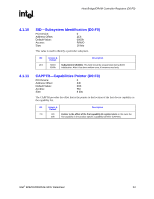
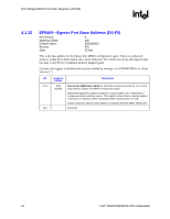
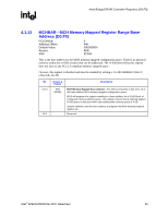
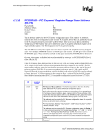
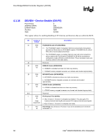
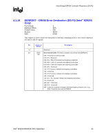
Host Bridge/DRAM Controller Registers (D0:F0) R 4.1.16 DEVEN-Device Enable (D0:F0) PCI Device: Address Offset: Default Value: Access: Size: 0 54h 00000019h R/W 32 bits This register allows for enabling/disabling of PCI devices and functions that are within the MCH. Bit Access & Default Description 31 R/W PCIEXBAR Enable (PCIEXBAREN): 0b 0 = The PCIEXBAR register is disabled. Memory read and write transactions proceed as if there were no PCIEXBAR register. PCIEXBAR bits 31:28 are R/W with no functionality behind them. 1 = The PCIEXBAR register is enabled. Memory read and write transactions whose address bits 31:28 match PCIEXBAR 31:28 will be translated to configuration reads and writes within the MCH. These translated cycles are routed as shown in the table above. 30 Reserved 29 R/W DMIBAR Enable (DMIBAREN): 0b 0 = DMIBAR is disabled and does not claim any memory. 1 = DMIBAR memory mapped accesses are claimed and decoded appropriately. 28 R/W MCHBAR Enable (MCHBAREN): 0b 0 = MCHBAR is disabled and does not claim any memory. 1 = MCHBAR memory mapped accesses are claimed and decoded appropriately. 27 R/W EPBAR Enable (EPBAREN): 0b 0 = EPBAR is disabled and does not claim any memory. 1 = EPBAR memory mapped accesses are claimed and decoded appropriately. 26:2 Reserved 1 R/W PCI Express* Port (D1EN): 1b 0 = Bus 0 Device 1 Function 0 is disabled and hidden. This also gates PCI Strap Express internal clock (lgclk) and asserts PCI Express internal reset (lgrstb). dependent 1 = Bus 0 Device 1 Function 0 is enabled and visible. 0 RO Host Bridge: Bus 0 Device 0 Function 0 can not be disabled and is therefore 1b hardwired to 1. 58 Intel® 82925X/82925XE MCH Datasheet
-
 1
1 -
2
-
3
-
4
-
5
-
6
-
7
-
8
-
9
-
10
-
11
-
12
-
13
-
14
-
15
-
16
-
17
-
18
-
19
-
20
-
21
-
22
-
23
-
24
-
25
-
26
-
27
-
28
-
29
-
30
-
31
-
32
-
33
-
34
-
35
-
36
-
37
-
38
-
39
-
40
-
41
-
42
-
43
-
44
-
45
-
46
-
47
-
48
-
49
-
50
-
51
-
52
-
 53
53 -
 54
54 -
 55
55 -
 56
56 -
 57
57 -
 58
58 -
 59
59 -
 60
60 -
 61
61 -
 62
62 -
 63
63 -
64
-
65
-
66
-
67
-
68
-
69
-
70
-
71
-
72
-
73
-
74
-
75
-
76
-
77
-
78
-
79
-
80
-
81
-
82
-
83
-
84
-
85
-
86
-
87
-
88
-
89
-
90
-
91
-
92
-
93
-
94
-
95
-
96
-
97
-
98
-
99
-
100
-
101
-
102
-
103
-
104
-
105
-
106
-
107
-
108
-
109
-
110
-
111
-
112
-
113
-
114
-
115
-
116
-
117
-
118
-
119
-
120
-
121
-
122
-
123
-
124
-
125
-
126
-
127
-
128
-
129
-
130
-
131
-
132
-
133
-
134
-
135
-
136
-
137
-
138
-
139
-
140
-
141
-
142
-
143
-
144
-
145
-
146
-
147
-
148
-
149
-
150
-
151
-
152
-
153
-
154
-
155
-
156
-
157
-
158
-
159
-
160
-
161
-
162
-
163
-
164
-
165
-
166
-
167
-
168
-
169
-
170
-
171
-
172
-
173
-
174
-
175
-
176
-
177
-
178
-
179
-
180
-
181
-
182
-
183
-
184
-
185
-
186
-
187
-
188
-
189
-
190
-
191
-
192
-
193
-
194
-
195
-
196
-
197
-
198
-
199
-
200
-
201
-
202
-
203
-
204
-
205
-
206
-
207
-
208
-
209
-
210
-
211
-
212
-
213
-
214
-
215
-
216
-
217
-
218
-
219
-
220
-
221
-
222
-
223
-
224
-
225
-
226
-
227
-
228
-
229
-
230
-
231
-
232
-
233
-
234
-
235
-
236
-
237
-
238
-
239
-
240
-
241
-
242
 |
 |