Intel 925 Data Sheet - Page 62
PAM0-Programmable Attribute Map 0 D0:F0, Warning
 |
UPC - 683728067724
View all Intel 925 manuals
Add to My Manuals
Save this manual to your list of manuals |
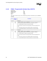
Page 62 highlights
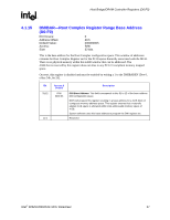
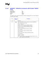
Host Bridge/DRAM Controller Registers (D0:F0) R 4.1.20 PAM0-Programmable Attribute Map 0 (D0:F0) PCI Device: Address Offset: Default Value: Access: Size: 0 90h 00h R/W 8 bits This register controls the read, write, and shadowing attributes of the BIOS area from 0F0000h- 0FFFFFh The MCH allows programmable memory attributes on 13 Legacy memory segments of various sizes in the 768-KB to 1-MB address range. Seven Programmable Attribute Map (PAM) Registers are used to support these features. Cache ability of these areas is controlled via the MTRR registers in the P6 processor. Two bits are used to specify memory attributes for each memory segment. These bits apply to both host accesses and PCI initiator accesses to the PAM areas. These attributes are: • RE (Read Enable). When RE = 1, the processor read accesses to the corresponding memory segment are claimed by the MCH and directed to main memory. Conversely, when RE = 0, the host read accesses are directed to Primary PCI. • WE (Write Enable). When WE = 1, the host write accesses to the corresponding memory segment are claimed by the MCH and directed to main memory. Conversely, when WE = 0, the host write accesses are directed to Primary PCI. The RE and WE attributes permit a memory segment to be Read Only, Write Only, Read/Write, or disabled. For example, if a memory segment has RE = 1 and WE = 0, the segment is Read Only. Each PAM Register controls two regions, typically 16 KB in size. Bit Access & Default Description 7:6 Reserved 5:4 R/W 0F0000-0FFFFF Attribute (HIENABLE): This field controls the steering of read and 00b write cycles that addresses the BIOS area from 0F0000h to 0FFFFFh. 00 = DRAM Disabled: All accesses are directed to the DMI. 01 = Read Only: All reads are sent to DRAM. All writes are forwarded to the DMI. 10 = Write Only: All writes are sent to DRAM. Reads are serviced by DMI. 11 = Normal DRAM Operation: All reads and writes are serviced by DRAM. 3:0 Reserved Warning: The MCH may hang if a PCI Express graphics attach or DMI originated access to Read Disabled or Write Disabled PAM segments occurs (due to a possible IWB to non-DRAM). For these reasons the following critical restriction is placed on the programming of the PAM regions: At the time that a DMI or PCI Express graphics attach accesses to the PAM region may occur, the targeted PAM segment must be programmed to be both readable and writeable. 62 Intel® 82925X/82925XE MCH Datasheet
-
 1
1 -
2
-
3
-
4
-
5
-
6
-
7
-
8
-
9
-
10
-
11
-
12
-
13
-
14
-
15
-
16
-
17
-
18
-
19
-
20
-
21
-
22
-
23
-
24
-
25
-
26
-
27
-
28
-
29
-
30
-
31
-
32
-
33
-
34
-
35
-
36
-
37
-
38
-
39
-
40
-
41
-
42
-
43
-
44
-
45
-
46
-
47
-
48
-
49
-
50
-
51
-
52
-
53
-
54
-
55
-
56
-
 57
57 -
 58
58 -
 59
59 -
 60
60 -
 61
61 -
 62
62 -
 63
63 -
 64
64 -
 65
65 -
 66
66 -
 67
67 -
68
-
69
-
70
-
71
-
72
-
73
-
74
-
75
-
76
-
77
-
78
-
79
-
80
-
81
-
82
-
83
-
84
-
85
-
86
-
87
-
88
-
89
-
90
-
91
-
92
-
93
-
94
-
95
-
96
-
97
-
98
-
99
-
100
-
101
-
102
-
103
-
104
-
105
-
106
-
107
-
108
-
109
-
110
-
111
-
112
-
113
-
114
-
115
-
116
-
117
-
118
-
119
-
120
-
121
-
122
-
123
-
124
-
125
-
126
-
127
-
128
-
129
-
130
-
131
-
132
-
133
-
134
-
135
-
136
-
137
-
138
-
139
-
140
-
141
-
142
-
143
-
144
-
145
-
146
-
147
-
148
-
149
-
150
-
151
-
152
-
153
-
154
-
155
-
156
-
157
-
158
-
159
-
160
-
161
-
162
-
163
-
164
-
165
-
166
-
167
-
168
-
169
-
170
-
171
-
172
-
173
-
174
-
175
-
176
-
177
-
178
-
179
-
180
-
181
-
182
-
183
-
184
-
185
-
186
-
187
-
188
-
189
-
190
-
191
-
192
-
193
-
194
-
195
-
196
-
197
-
198
-
199
-
200
-
201
-
202
-
203
-
204
-
205
-
206
-
207
-
208
-
209
-
210
-
211
-
212
-
213
-
214
-
215
-
216
-
217
-
218
-
219
-
220
-
221
-
222
-
223
-
224
-
225
-
226
-
227
-
228
-
229
-
230
-
231
-
232
-
233
-
234
-
235
-
236
-
237
-
238
-
239
-
240
-
241
-
242
 |
 |