Intel 925 Data Sheet - Page 7

Processor WB Transaction to an Enabled SMM Address Space, Legacy VGA and I/O Range Decode Rules - drivers

Page 7 highlights

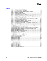
R 9.3.3 FSB Interrupt Memory Space (FEE0_0000h-FEEF_FFFFh 165 9.3.4 High BIOS Area 165 9.3.5 PCI Express* Configuration Address Space 165 9.3.6 PCI Express* Graphics Attach 166 9.3.7 AGP DRAM Graphics Aperture 166 9.4 System Management Mode (SMM 167 9.4.1 SMM Space Definition 167 9.4.2 SMM Space Restrictions 168 9.4.3 SMM Space Combinations 168 9.4.4 SMM Control Combinations 169 9.4.5 SMM Space Decode and Transaction Handling 169 9.4.6 Processor WB Transaction to an Enabled SMM Address Space ...... 169 9.4.7 SMM Access through GTT TLB 170 9.4.8 Memory Shadowing 170 9.4.9 I/O Address Space 170 9.4.10 PCI Express* I/O Address Mapping 171 9.4.11 MCH Decode Rules and Cross-Bridge Address Mapping 171 9.4.12 Legacy VGA and I/O Range Decode Rules 171 10 Functional Description ...173 10.1 Host Interface ...173 10.1.1 FSB GTL+ Termination 173 10.1.2 FSB Dynamic Bus Inversion 173 10.1.3 APIC Cluster Mode Support 174 10.2 System Memory Controller 174 10.2.1 Memory Organization Modes 174 10.3 System Memory Configuration Register Overview 176 10.3.1 DRAM Technologies and Organization 177 10.3.1.1 Rules for Populating DIMM Slots 177 10.3.1.2 System Memory Supported Configurations 178 10.3.1.3 Main Memory DRAM Address Translation and Decoding 178 10.3.2 DRAM Clock Generation 181 10.3.3 Suspend to RAM and Resume 181 10.3.4 DDR2 On-Die Termination 181 10.3.5 DDR2 Off-Chip Driver Impedance Calibration 181 10.4 PCI Express* ...182 10.4.1 Transaction Layer 182 10.4.2 Data Link Layer 182 10.4.3 Physical Layer 182 10.5 Power Management 183 10.6 Clocking...183 11 Electrical Characteristics 185 11.1 Absolute Maximum Ratings 185 11.2 Power Characteristics 186 11.3 Signal Groups...187 11.4 General DC Characteristics 189 12 Ballout and Package Information 193 12.1 Ballout...193 12.2 Package Information 219 Intel® 82925X/82925XE MCH Datasheet 7

  • 1
  • 2
  • 3
  • 4
  • 5
  • 6
  • 7
  • 8
  • 9
  • 10
  • 11
  • 12
  • 13
  • 14
  • 15
  • 16
  • 17
  • 18
  • 19
  • 20
  • 21
  • 22
  • 23
  • 24
  • 25
  • 26
  • 27
  • 28
  • 29
  • 30
  • 31
  • 32
  • 33
  • 34
  • 35
  • 36
  • 37
  • 38
  • 39
  • 40
  • 41
  • 42
  • 43
  • 44
  • 45
  • 46
  • 47
  • 48
  • 49
  • 50
  • 51
  • 52
  • 53
  • 54
  • 55
  • 56
  • 57
  • 58
  • 59
  • 60
  • 61
  • 62
  • 63
  • 64
  • 65
  • 66
  • 67
  • 68
  • 69
  • 70
  • 71
  • 72
  • 73
  • 74
  • 75
  • 76
  • 77
  • 78
  • 79
  • 80
  • 81
  • 82
  • 83
  • 84
  • 85
  • 86
  • 87
  • 88
  • 89
  • 90
  • 91
  • 92
  • 93
  • 94
  • 95
  • 96
  • 97
  • 98
  • 99
  • 100
  • 101
  • 102
  • 103
  • 104
  • 105
  • 106
  • 107
  • 108
  • 109
  • 110
  • 111
  • 112
  • 113
  • 114
  • 115
  • 116
  • 117
  • 118
  • 119
  • 120
  • 121
  • 122
  • 123
  • 124
  • 125
  • 126
  • 127
  • 128
  • 129
  • 130
  • 131
  • 132
  • 133
  • 134
  • 135
  • 136
  • 137
  • 138
  • 139
  • 140
  • 141
  • 142
  • 143
  • 144
  • 145
  • 146
  • 147
  • 148
  • 149
  • 150
  • 151
  • 152
  • 153
  • 154
  • 155
  • 156
  • 157
  • 158
  • 159
  • 160
  • 161
  • 162
  • 163
  • 164
  • 165
  • 166
  • 167
  • 168
  • 169
  • 170
  • 171
  • 172
  • 173
  • 174
  • 175
  • 176
  • 177
  • 178
  • 179
  • 180
  • 181
  • 182
  • 183
  • 184
  • 185
  • 186
  • 187
  • 188
  • 189
  • 190
  • 191
  • 192
  • 193
  • 194
  • 195
  • 196
  • 197
  • 198
  • 199
  • 200
  • 201
  • 202
  • 203
  • 204
  • 205
  • 206
  • 207
  • 208
  • 209
  • 210
  • 211
  • 212
  • 213
  • 214
  • 215
  • 216
  • 217
  • 218
  • 219
  • 220
  • 221
  • 222
  • 223
  • 224
  • 225
  • 226
  • 227
  • 228
  • 229
  • 230
  • 231
  • 232
  • 233
  • 234
  • 235
  • 236
  • 237
  • 238
  • 239
  • 240
  • 241
  • 242

R
Intel
®
82925X/82925XE MCH Datasheet
7
9.3.3
FSB Interrupt Memory Space (FEE0_0000h–FEEF_FFFFh)
............
165
9.3.4
High BIOS Area
..................................................................................
165
9.3.5
PCI Express* Configuration Address Space
......................................
165
9.3.6
PCI Express* Graphics Attach
............................................................
166
9.3.7
AGP DRAM Graphics Aperture
..........................................................
166
9.4
System Management Mode (SMM)
...................................................................
167
9.4.1
SMM Space Definition
........................................................................
167
9.4.2
SMM Space Restrictions
....................................................................
168
9.4.3
SMM Space Combinations
.................................................................
168
9.4.4
SMM Control Combinations
................................................................
169
9.4.5
SMM Space Decode and Transaction Handling
................................
169
9.4.6
Processor WB Transaction to an Enabled SMM Address Space
......
169
9.4.7
SMM Access through GTT TLB
..........................................................
170
9.4.8
Memory Shadowing
............................................................................
170
9.4.9
I/O Address Space
..............................................................................
170
9.4.10
PCI Express* I/O Address Mapping
...................................................
171
9.4.11
MCH Decode Rules and Cross-Bridge Address Mapping
.................
171
9.4.12
Legacy VGA and I/O Range Decode Rules
.......................................
171
10
Functional Description
....................................................................................................
173
10.1
Host Interface
.....................................................................................................
173
10.1.1
FSB GTL+ Termination
.......................................................................
173
10.1.2
FSB Dynamic Bus Inversion
...............................................................
173
10.1.3
APIC Cluster Mode Support
...............................................................
174
10.2
System Memory Controller
.................................................................................
174
10.2.1
Memory Organization Modes
..............................................................
174
10.3
System Memory Configuration Register Overview
............................................
176
10.3.1
DRAM Technologies and Organization
..............................................
177
10.3.1.1
Rules for Populating DIMM Slots
......................................
177
10.3.1.2
System Memory Supported Configurations
......................
178
10.3.1.3
Main Memory DRAM Address Translation and Decoding 178
10.3.2
DRAM Clock Generation
....................................................................
181
10.3.3
Suspend to RAM and Resume
...........................................................
181
10.3.4
DDR2 On-Die Termination
..................................................................
181
10.3.5
DDR2 Off-Chip Driver Impedance Calibration
....................................
181
10.4
PCI Express*
......................................................................................................
182
10.4.1
Transaction Layer
...............................................................................
182
10.4.2
Data Link Layer
...................................................................................
182
10.4.3
Physical Layer
.....................................................................................
182
10.5
Power Management
...........................................................................................
183
10.6
Clocking
..............................................................................................................
183
11
Electrical Characteristics
.................................................................................................
185
11.1
Absolute Maximum Ratings
................................................................................
185
11.2
Power Characteristics
........................................................................................
186
11.3
Signal Groups
.....................................................................................................
187
11.4
General DC Characteristics
...............................................................................
189
12
Ballout and Package Information
....................................................................................
193
12.1
Ballout
.................................................................................................................
193
12.2
Package Information
..........................................................................................
219