Intel 925 Data Sheet - Page 71
SMRAM-System Management RAM Control D0:F0, PCI Device, Address Offset, Default Value, Access, R/W/L
 |
UPC - 683728067724
View all Intel 925 manuals
Add to My Manuals
Save this manual to your list of manuals |
Page 71 highlights
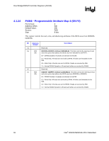
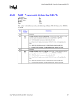
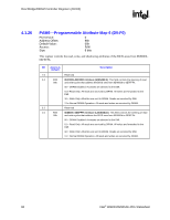
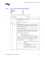
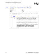
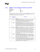
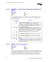
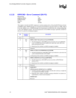
Host Bridge/DRAM Controller Registers (D0:F0) R 4.1.29 SMRAM-System Management RAM Control (D0:F0) PCI Device: Address Offset: Default Value: Access: Size: 0 9Dh 00h R/W/L, RO 8 bits The SMRAMC register controls how accesses to Compatible and Extended SMRAM spaces are treated. The Open, Close, and Lock bits function only when G_SMRAME bit is set to a 1. Also, the OPEN bit must be reset before the LOCK bit is set. Bit Access & Default Description 7 Reserved 6 R/W/L SMM Space Open (D_OPEN): When D_OPEN=1 and D_LCK=0, the SMM 0b space DRAM is made visible even when SMM decode is not active. This is intended to help BIOS initialize SMM space. Software should ensure that D_OPEN=1 and D_CLS=1 are not set at the same time. 5 R/W/L SMM Space Closed (D_CLS): When D_CLS = 1 SMM space DRAM is not 0b accessible to data references, even if SMM decode is active. Code references may still access SMM space DRAM. This will allow SMM software to reference through SMM space to update the display even when SMM is mapped over the VGA range. Software should ensure that D_OPEN=1 and D_CLS=1 are not set at the same time. Note that the D_CLS bit only applies to Compatible SMM space. 4 R/W/L SMM Space Locked (D_LCK): When D_LCK is set to 1, D_OPEN is reset to 0 0b and D_LCK, D_OPEN, C_BASE_SEG, H_SMRAM_EN, TSEG_SZ and TSEG_EN become read only. D_LCK can be set to 1 via a normal configuration space write but can only be cleared by a full Reset. The combination of D_LCK and D_OPEN provide convenience with security. The BIOS can use the D_OPEN function to initialize SMM space and then use D_LCK to "lock down" SMM space in the future so that no application software (or BIOS itself) can violate the integrity of SMM space, even if the program has knowledge of the D_OPEN function. 3 R/W/L Global SMRAM Enable (G_SMRAME): If set to a 1, Compatible SMRAM 0b functions are enabled, providing 128 KB of DRAM accessible at the A0000h address while in SMM (ADSB with SMM decode). To enable Extended SMRAM function this bit has be set to 1. Refer to the section on SMM for more details. Once D_LCK is set, this bit becomes read only. 2:0 RO Compatible SMM Space Base Segment (C_BASE_SEG): This field indicates 010b the location of SMM space. SMM DRAM is not remapped. It is simply made visible if the conditions are right to access SMM space, otherwise the access is forwarded to DMI. Since the MCH supports only the SMM space between A0000h and BFFFFh, this field is hardwired to 010. Intel® 82925X/82925XE MCH Datasheet 71
-
 1
1 -
2
-
3
-
4
-
5
-
6
-
7
-
8
-
9
-
10
-
11
-
12
-
13
-
14
-
15
-
16
-
17
-
18
-
19
-
20
-
21
-
22
-
23
-
24
-
25
-
26
-
27
-
28
-
29
-
30
-
31
-
32
-
33
-
34
-
35
-
36
-
37
-
38
-
39
-
40
-
41
-
42
-
43
-
44
-
45
-
46
-
47
-
48
-
49
-
50
-
51
-
52
-
53
-
54
-
55
-
56
-
57
-
58
-
59
-
60
-
61
-
62
-
63
-
64
-
65
-
 66
66 -
 67
67 -
 68
68 -
 69
69 -
 70
70 -
 71
71 -
 72
72 -
 73
73 -
 74
74 -
 75
75 -
 76
76 -
77
-
78
-
79
-
80
-
81
-
82
-
83
-
84
-
85
-
86
-
87
-
88
-
89
-
90
-
91
-
92
-
93
-
94
-
95
-
96
-
97
-
98
-
99
-
100
-
101
-
102
-
103
-
104
-
105
-
106
-
107
-
108
-
109
-
110
-
111
-
112
-
113
-
114
-
115
-
116
-
117
-
118
-
119
-
120
-
121
-
122
-
123
-
124
-
125
-
126
-
127
-
128
-
129
-
130
-
131
-
132
-
133
-
134
-
135
-
136
-
137
-
138
-
139
-
140
-
141
-
142
-
143
-
144
-
145
-
146
-
147
-
148
-
149
-
150
-
151
-
152
-
153
-
154
-
155
-
156
-
157
-
158
-
159
-
160
-
161
-
162
-
163
-
164
-
165
-
166
-
167
-
168
-
169
-
170
-
171
-
172
-
173
-
174
-
175
-
176
-
177
-
178
-
179
-
180
-
181
-
182
-
183
-
184
-
185
-
186
-
187
-
188
-
189
-
190
-
191
-
192
-
193
-
194
-
195
-
196
-
197
-
198
-
199
-
200
-
201
-
202
-
203
-
204
-
205
-
206
-
207
-
208
-
209
-
210
-
211
-
212
-
213
-
214
-
215
-
216
-
217
-
218
-
219
-
220
-
221
-
222
-
223
-
224
-
225
-
226
-
227
-
228
-
229
-
230
-
231
-
232
-
233
-
234
-
235
-
236
-
237
-
238
-
239
-
240
-
241
-
242
 |
 |