Intel 925 Data Sheet - Page 72
ESMRAMC-Extended System Management RAM Control, D0:F0, ERRSTS-Error Status D0:F0, PCI Device
 |
UPC - 683728067724
View all Intel 925 manuals
Add to My Manuals
Save this manual to your list of manuals |
Page 72 highlights
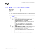
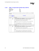
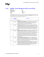
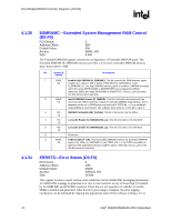
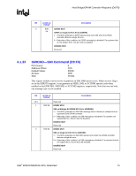
Host Bridge/DRAM Controller Registers (D0:F0) R 4.1.30 ESMRAMC-Extended System Management RAM Control (D0:F0) PCI Device: Address Offset: Default Value: Access: Size: 0 9Eh 00h R/W/L, RO 8 bits The Extended SMRAM register controls the configuration of Extended SMRAM space. The Extended SMRAM (E_SMRAM) memory provides a write-back cacheable SMRAM memory space that is above 1 MB. Bit Access & Default Description 7 R/W/L Enable High SMRAM (H_SMRAME): This bit controls the SMM memory space 0b location (i.e., above 1 MB or below 1 MB) When G_SMRAME is 1 and H_SMRAME is 1, the high SMRAM memory space is enabled. SMRAM accesses within the range 0FEDA0000h to 0FEDBFFFFh are remapped to DRAM addresses within the range 000A0000h to 000BFFFFh. Once D_LCK has been set, this bit becomes read only. 6 R/W/C Invalid SMRAM Access (E_SMERR): This bit is set when the processor has 0b accessed the defined memory ranges in Extended SMRAM (High Memory and T- segment) while not in SMM space and with the D-OPEN bit = 0. It is software's responsibility to clear this bit. The software must write a 1 to this bit to clear it. 5 RO SMRAM Cacheable (SM_CACHE): This bit is forced to 1 by the MCH . 1b 4 RO L1 Cache Enable for SMRAM (SM_L1): This bit is forced to 1 by the MCH. 1b 3 RO L2 Cache Enable for SMRAM (SM_L2): This bit is forced to 1 by the MCH. 1b 2:1 Reserved 0 R/W/L TSEG Enable (T_EN): This bit Enables SMRAM memory for Extended SMRAM 0b space only. When G_SMRAME =1 and TSEG_EN = 1, the TSEG is enabled to appear in the appropriate physical address space. Note that once D_LCK is set, this bit becomes read only. 4.1.31 ERRSTS-Error Status (D0:F0) PCI Device: Address Offset: Default Value: Access: Size: 0 C8h 0000h R/WC/S, RO 16 bits This register is used to report various error conditions via the SERR DMI messaging mechanism. An SERR DMI message is generated on a zero to one transition of any of these flags (if enabled by the ERRCMD and PCICMD registers). These bits are set regardless of whether or not the SERR is enabled and generated. After the error processing is complete, the error logging mechanism can be unlocked by clearing the appropriate status bit by software writing a 1 to it. 72 Intel® 82925X/82925XE MCH Datasheet
-
 1
1 -
2
-
3
-
4
-
5
-
6
-
7
-
8
-
9
-
10
-
11
-
12
-
13
-
14
-
15
-
16
-
17
-
18
-
19
-
20
-
21
-
22
-
23
-
24
-
25
-
26
-
27
-
28
-
29
-
30
-
31
-
32
-
33
-
34
-
35
-
36
-
37
-
38
-
39
-
40
-
41
-
42
-
43
-
44
-
45
-
46
-
47
-
48
-
49
-
50
-
51
-
52
-
53
-
54
-
55
-
56
-
57
-
58
-
59
-
60
-
61
-
62
-
63
-
64
-
65
-
66
-
 67
67 -
 68
68 -
 69
69 -
 70
70 -
 71
71 -
 72
72 -
 73
73 -
 74
74 -
 75
75 -
 76
76 -
 77
77 -
78
-
79
-
80
-
81
-
82
-
83
-
84
-
85
-
86
-
87
-
88
-
89
-
90
-
91
-
92
-
93
-
94
-
95
-
96
-
97
-
98
-
99
-
100
-
101
-
102
-
103
-
104
-
105
-
106
-
107
-
108
-
109
-
110
-
111
-
112
-
113
-
114
-
115
-
116
-
117
-
118
-
119
-
120
-
121
-
122
-
123
-
124
-
125
-
126
-
127
-
128
-
129
-
130
-
131
-
132
-
133
-
134
-
135
-
136
-
137
-
138
-
139
-
140
-
141
-
142
-
143
-
144
-
145
-
146
-
147
-
148
-
149
-
150
-
151
-
152
-
153
-
154
-
155
-
156
-
157
-
158
-
159
-
160
-
161
-
162
-
163
-
164
-
165
-
166
-
167
-
168
-
169
-
170
-
171
-
172
-
173
-
174
-
175
-
176
-
177
-
178
-
179
-
180
-
181
-
182
-
183
-
184
-
185
-
186
-
187
-
188
-
189
-
190
-
191
-
192
-
193
-
194
-
195
-
196
-
197
-
198
-
199
-
200
-
201
-
202
-
203
-
204
-
205
-
206
-
207
-
208
-
209
-
210
-
211
-
212
-
213
-
214
-
215
-
216
-
217
-
218
-
219
-
220
-
221
-
222
-
223
-
224
-
225
-
226
-
227
-
228
-
229
-
230
-
231
-
232
-
233
-
234
-
235
-
236
-
237
-
238
-
239
-
240
-
241
-
242
 |
 |
