Intel 925 Data Sheet - Page 74
ERRCMD-Error Command D0:F0
 |
UPC - 683728067724
View all Intel 925 manuals
Add to My Manuals
Save this manual to your list of manuals |
Page 74 highlights
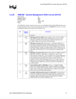
Host Bridge/DRAM Controller Registers (D0:F0) R 4.1.32 ERRCMD-Error Command (D0:F0) PCI Device: Address Offset: Default Value: Access: Size: 0 CAh 0000h R/W 16 bits This register controls the MCH responses to various system errors. Since the MCH does not have an SERR# signal, SERR messages are passed from the MCH to the Intel ICH6 over DMI. When a bit in this register is set, a SERR message will be generated on DMI when the corresponding flag is set in the ERRSTS register. The actual generation of the SERR message is globally enabled for Device 0 via the PCI Command register. Bit 15:12 11 10 9 8 7:2 1 Access & Default Description Reserved R/W SERR on MCH Thermal Sensor Event (TSESERR) 0b 1 = The MCH generates a DMI SERR special cycle when bit 11 of the ERRSTS is set. The SERR must not be enabled at the same time as the SMI for the same thermal sensor event. 0 = Reporting of this condition via SERR messaging is disabled. Reserved R/W SERR on LOCK to non-DRAM Memory (LCKERR) 0b 1 = The MCH will generate a DMI SERR special cycle whenever a processor lock cycle is detected that does not hit DRAM. 0 = Reporting of this condition via SERR messaging is disabled. R/W SERR on DRAM Refresh Timeout (DRTOERR) 0b 1 = The MCH generates a DMI SERR special cycle when a DRAM Refresh timeout occurs. 0 = Reporting of this condition via SERR messaging is disabled. Reserved R/W 82925X MCH 0b SERR Multiple-Bit DRAM ECC Error (DMERR) 1 = The MCH generates a SERR message over DMI when it detects a multiple-bit error reported by the DRAM controller. 0 = Reporting of this condition via SERR messaging is disabled. For systems not supporting ECC, this bit must be disabled. 82925XE MCH Reserved 74 Intel® 82925X/82925XE MCH Datasheet
-
 1
1 -
2
-
3
-
4
-
5
-
6
-
7
-
8
-
9
-
10
-
11
-
12
-
13
-
14
-
15
-
16
-
17
-
18
-
19
-
20
-
21
-
22
-
23
-
24
-
25
-
26
-
27
-
28
-
29
-
30
-
31
-
32
-
33
-
34
-
35
-
36
-
37
-
38
-
39
-
40
-
41
-
42
-
43
-
44
-
45
-
46
-
47
-
48
-
49
-
50
-
51
-
52
-
53
-
54
-
55
-
56
-
57
-
58
-
59
-
60
-
61
-
62
-
63
-
64
-
65
-
66
-
67
-
68
-
 69
69 -
 70
70 -
 71
71 -
 72
72 -
 73
73 -
 74
74 -
 75
75 -
 76
76 -
 77
77 -
 78
78 -
 79
79 -
80
-
81
-
82
-
83
-
84
-
85
-
86
-
87
-
88
-
89
-
90
-
91
-
92
-
93
-
94
-
95
-
96
-
97
-
98
-
99
-
100
-
101
-
102
-
103
-
104
-
105
-
106
-
107
-
108
-
109
-
110
-
111
-
112
-
113
-
114
-
115
-
116
-
117
-
118
-
119
-
120
-
121
-
122
-
123
-
124
-
125
-
126
-
127
-
128
-
129
-
130
-
131
-
132
-
133
-
134
-
135
-
136
-
137
-
138
-
139
-
140
-
141
-
142
-
143
-
144
-
145
-
146
-
147
-
148
-
149
-
150
-
151
-
152
-
153
-
154
-
155
-
156
-
157
-
158
-
159
-
160
-
161
-
162
-
163
-
164
-
165
-
166
-
167
-
168
-
169
-
170
-
171
-
172
-
173
-
174
-
175
-
176
-
177
-
178
-
179
-
180
-
181
-
182
-
183
-
184
-
185
-
186
-
187
-
188
-
189
-
190
-
191
-
192
-
193
-
194
-
195
-
196
-
197
-
198
-
199
-
200
-
201
-
202
-
203
-
204
-
205
-
206
-
207
-
208
-
209
-
210
-
211
-
212
-
213
-
214
-
215
-
216
-
217
-
218
-
219
-
220
-
221
-
222
-
223
-
224
-
225
-
226
-
227
-
228
-
229
-
230
-
231
-
232
-
233
-
234
-
235
-
236
-
237
-
238
-
239
-
240
-
241
-
242
 |
 |