Intel 925 Data Sheet - Page 83
C0DRA0-Channel A DRAM Rank 0, 1 Attribute, DRAM Rank Attribute Registers, CxDRA, Channel and Rank Map
 |
UPC - 683728067724
View all Intel 925 manuals
Add to My Manuals
Save this manual to your list of manuals |
Page 83 highlights
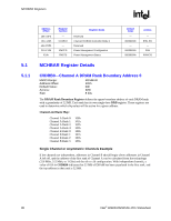
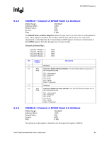
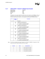
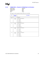
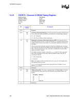
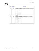
MCHBAR Registers R 5.1.5 5.1.6 C0DRA0-Channel A DRAM Rank 0,1 Attribute MMIO Range: Address Offset: Default Value: Access: Size: MCHBAR 108h 00h R/W 8 bits The DRAM Rank Attribute Registers define the page sizes to be used when accessing different ranks. These registers should be left with their default value (all zeros) for any rank that is unpopulated, as determined by the corresponding CxDRB registers. Each byte of information in the CxDRA registers describes the page size of a pair of ranks. Channel and Rank Map: Channel A Rank 0, 1: Channel A Rank 2, 3: Channel B Rank 0, 1: Channel B Rank 2, 3: 108h 109h 188h 189h Bit Access & Default Description 7 Reserved 6:4 R/W Channel A DRAM odd Rank Attribute: This 3 bit field defines the page size of 000b the corresponding rank. 000 = Unpopulated 001 = Reserved 010 = 4 KB 011 = 8 KB 100 = 16 KB Others = Reserved 3 Reserved 2:0 R/W Channel A DRAM even Rank Attribute: This 3 bit field defines the page size of 000b the corresponding rank. 000 = Unpopulated 001 = Reserved 010 = 4 KB 011 = 8 KB 100 = 16 KB Others = Reserved C0DRA2-Channel A DRAM Rank 2,3 Attribute MMIO Range: Address Offset: Default Value: Access: Size: MCHBAR 109h 00h R/W 8 bits The operation of this register is detailed in the description for register C0DRA0. Intel® 82925X/82925XE MCH Datasheet 83
-
 1
1 -
2
-
3
-
4
-
5
-
6
-
7
-
8
-
9
-
10
-
11
-
12
-
13
-
14
-
15
-
16
-
17
-
18
-
19
-
20
-
21
-
22
-
23
-
24
-
25
-
26
-
27
-
28
-
29
-
30
-
31
-
32
-
33
-
34
-
35
-
36
-
37
-
38
-
39
-
40
-
41
-
42
-
43
-
44
-
45
-
46
-
47
-
48
-
49
-
50
-
51
-
52
-
53
-
54
-
55
-
56
-
57
-
58
-
59
-
60
-
61
-
62
-
63
-
64
-
65
-
66
-
67
-
68
-
69
-
70
-
71
-
72
-
73
-
74
-
75
-
76
-
77
-
 78
78 -
 79
79 -
 80
80 -
 81
81 -
 82
82 -
 83
83 -
 84
84 -
 85
85 -
 86
86 -
 87
87 -
 88
88 -
89
-
90
-
91
-
92
-
93
-
94
-
95
-
96
-
97
-
98
-
99
-
100
-
101
-
102
-
103
-
104
-
105
-
106
-
107
-
108
-
109
-
110
-
111
-
112
-
113
-
114
-
115
-
116
-
117
-
118
-
119
-
120
-
121
-
122
-
123
-
124
-
125
-
126
-
127
-
128
-
129
-
130
-
131
-
132
-
133
-
134
-
135
-
136
-
137
-
138
-
139
-
140
-
141
-
142
-
143
-
144
-
145
-
146
-
147
-
148
-
149
-
150
-
151
-
152
-
153
-
154
-
155
-
156
-
157
-
158
-
159
-
160
-
161
-
162
-
163
-
164
-
165
-
166
-
167
-
168
-
169
-
170
-
171
-
172
-
173
-
174
-
175
-
176
-
177
-
178
-
179
-
180
-
181
-
182
-
183
-
184
-
185
-
186
-
187
-
188
-
189
-
190
-
191
-
192
-
193
-
194
-
195
-
196
-
197
-
198
-
199
-
200
-
201
-
202
-
203
-
204
-
205
-
206
-
207
-
208
-
209
-
210
-
211
-
212
-
213
-
214
-
215
-
216
-
217
-
218
-
219
-
220
-
221
-
222
-
223
-
224
-
225
-
226
-
227
-
228
-
229
-
230
-
231
-
232
-
233
-
234
-
235
-
236
-
237
-
238
-
239
-
240
-
241
-
242
 |
 |