Intel 925 Data Sheet - Page 84
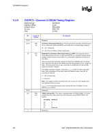
C0DCLKDIS-Channel A DRAM Clock Disable
 |
UPC - 683728067724
View all Intel 925 manuals
Add to My Manuals
Save this manual to your list of manuals |
Page 84 highlights
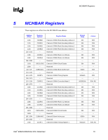
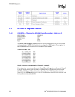
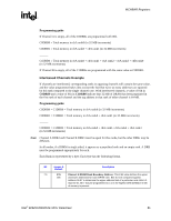
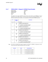
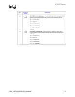
MCHBAR Registers R 5.1.7 C0DCLKDIS-Channel A DRAM Clock Disable MMIO Range: Address Offset: Default Value: Access: Size: MCHBAR 10Ch 00h R/W 8 bits This register can be used to disable the system memory clock signals to each DIMM slot. This can significantly reduce EMI and Power concerns for clocks that go to unpopulated DIMMs. Clocks should be enabled based on whether a slot is populated, and what kind of DIMM is present. Bit Access & Default Description 7:6 Reserved 5 R/W DIMM Clock Gate Enable Pair 5 0b 0 = Tri-state the corresponding clock pair. 1 = Enable the corresponding clock pair. 4 R/W DIMM Clock Gate Enable Pair 4 0b 0 = Tri-state the corresponding clock pair. 1 = Enable the corresponding clock pair. 3 R/W DIMM Clock Gate Enable Pair 3 0b 0 = Tri-state the corresponding clock pair. 1 = Enable the corresponding clock pair. 2 R/W DIMM Clock Gate Enable Pair 2 0b 0 = Tri-state the corresponding clock pair. 1 = Enable the corresponding clock pair. 1 R/W DIMM Clock Gate Enable Pair 1 0b 0 = Tri-state the corresponding clock pair. 1 = Enable the corresponding clock pair. 0 R/W DIMM Clock Gate Enable Pair 0 0b 0 = Tri-state the corresponding clock pair. 1 = Enable the corresponding clock pair. Note: Since there are multiple clock signals assigned to each Rank of a DIMM, it is important to clarify exactly which Rank width field affects which clock signal: Channel 0 0 1 1 Rank 0 or 1 2 or 3 0 or 1 2 or 3 Clocks Affected SCLK_A[2:0]/ SCLK_A[2:0]# SCLK_A[5:3]/ SCLK_A[5:3]# SCLK_B[2:0]/ SCLK_B[2:0]# SCLK_B[5:3]/ SCLK_B[5:3]# 84 Intel® 82925X/82925XE MCH Datasheet
-
 1
1 -
2
-
3
-
4
-
5
-
6
-
7
-
8
-
9
-
10
-
11
-
12
-
13
-
14
-
15
-
16
-
17
-
18
-
19
-
20
-
21
-
22
-
23
-
24
-
25
-
26
-
27
-
28
-
29
-
30
-
31
-
32
-
33
-
34
-
35
-
36
-
37
-
38
-
39
-
40
-
41
-
42
-
43
-
44
-
45
-
46
-
47
-
48
-
49
-
50
-
51
-
52
-
53
-
54
-
55
-
56
-
57
-
58
-
59
-
60
-
61
-
62
-
63
-
64
-
65
-
66
-
67
-
68
-
69
-
70
-
71
-
72
-
73
-
74
-
75
-
76
-
77
-
78
-
 79
79 -
 80
80 -
 81
81 -
 82
82 -
 83
83 -
 84
84 -
 85
85 -
 86
86 -
 87
87 -
 88
88 -
 89
89 -
90
-
91
-
92
-
93
-
94
-
95
-
96
-
97
-
98
-
99
-
100
-
101
-
102
-
103
-
104
-
105
-
106
-
107
-
108
-
109
-
110
-
111
-
112
-
113
-
114
-
115
-
116
-
117
-
118
-
119
-
120
-
121
-
122
-
123
-
124
-
125
-
126
-
127
-
128
-
129
-
130
-
131
-
132
-
133
-
134
-
135
-
136
-
137
-
138
-
139
-
140
-
141
-
142
-
143
-
144
-
145
-
146
-
147
-
148
-
149
-
150
-
151
-
152
-
153
-
154
-
155
-
156
-
157
-
158
-
159
-
160
-
161
-
162
-
163
-
164
-
165
-
166
-
167
-
168
-
169
-
170
-
171
-
172
-
173
-
174
-
175
-
176
-
177
-
178
-
179
-
180
-
181
-
182
-
183
-
184
-
185
-
186
-
187
-
188
-
189
-
190
-
191
-
192
-
193
-
194
-
195
-
196
-
197
-
198
-
199
-
200
-
201
-
202
-
203
-
204
-
205
-
206
-
207
-
208
-
209
-
210
-
211
-
212
-
213
-
214
-
215
-
216
-
217
-
218
-
219
-
220
-
221
-
222
-
223
-
224
-
225
-
226
-
227
-
228
-
229
-
230
-
231
-
232
-
233
-
234
-
235
-
236
-
237
-
238
-
239
-
240
-
241
-
242
 |
 |