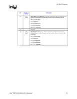
Intel 925 Data Sheet - Page 89
Mode Select SMS., DRAM Type DT., Second Revision Dual Data Rate DDR2 SDRAM
 |
UPC - 683728067724
View all Intel 925 manuals
Add to My Manuals
Save this manual to your list of manuals |
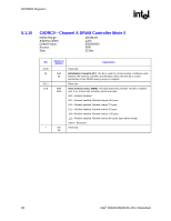
Page 89 highlights
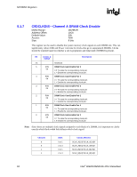
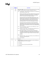
MCHBAR Registers R Bit Access & Default Description 6:4 R/W Mode Select (SMS). These bits select the special operational mode of the DRAM 000 b interface. The special modes are intended for initialization at power up. 000 = Post Reset state - When the MCH exits reset (power-up or otherwise), the mode select field is cleared to "000". During any reset sequence, while power is applied and reset is active, the MCH de-asserts all CKE signals. After internal reset is de-asserted, CKE signals remain de-asserted until this field is written to a value different than "000". On this event, all CKE signals are asserted. During suspend, MCH internal signal triggers DRAM controller to flush pending commands and enter all ranks into Self-Refresh mode. As part of resume sequence, MCH will be reset - which will clear this bit field to "000" and maintain CKE signals de-asserted. After internal reset is deasserted, CKE signals remain de-asserted until this field is written to a value different than "000". On this event, all CKE signals are asserted. During entry to other low power states (C3, S1), MCH internal signal triggers DRAM controller to flush pending commands and enter all ranks into Self-Refresh mode. During exit to normal mode, MCH signal triggers DRAM controller to exit Self-Refresh and resume normal operation without S/W involvement. 001 = NOP Command Enable - All processor cycles to DRAM result in a NOP command on the DRAM interface. 010 = All Banks Pre-charge Enable - All processor cycles to DRAM result in an "all banks precharge" command on the DRAM interface. 011 = Mode Register Set Enable - All processor cycles to DRAM result in a "mode register" set command on the DRAM interface. Host address lines are mapped to DRAM address lines in order to specify the command sent. Host address lines [12:3] are mapped to MA[9:0], and HA[13] is mapped to MA[11]. 101 = Reserved 110 = CBR Refresh Enable - In this mode all processor cycles to DRAM result in a CBR cycle on the DRAM interface 111 = Normal operation 3:2 Reserved 1:0 RO DRAM Type (DT). This field is used to select between supported SDRAM types. This bit is controlled by the MTYPE strap signal. 00 = Reserved 01 = Reserved 10 = Second Revision Dual Data Rate (DDR2) SDRAM 11 = Reserved Intel® 82925X/82925XE MCH Datasheet 89
-
 1
1 -
2
-
3
-
4
-
5
-
6
-
7
-
8
-
9
-
10
-
11
-
12
-
13
-
14
-
15
-
16
-
17
-
18
-
19
-
20
-
21
-
22
-
23
-
24
-
25
-
26
-
27
-
28
-
29
-
30
-
31
-
32
-
33
-
34
-
35
-
36
-
37
-
38
-
39
-
40
-
41
-
42
-
43
-
44
-
45
-
46
-
47
-
48
-
49
-
50
-
51
-
52
-
53
-
54
-
55
-
56
-
57
-
58
-
59
-
60
-
61
-
62
-
63
-
64
-
65
-
66
-
67
-
68
-
69
-
70
-
71
-
72
-
73
-
74
-
75
-
76
-
77
-
78
-
79
-
80
-
81
-
82
-
83
-
 84
84 -
 85
85 -
 86
86 -
 87
87 -
 88
88 -
 89
89 -
 90
90 -
 91
91 -
 92
92 -
 93
93 -
 94
94 -
95
-
96
-
97
-
98
-
99
-
100
-
101
-
102
-
103
-
104
-
105
-
106
-
107
-
108
-
109
-
110
-
111
-
112
-
113
-
114
-
115
-
116
-
117
-
118
-
119
-
120
-
121
-
122
-
123
-
124
-
125
-
126
-
127
-
128
-
129
-
130
-
131
-
132
-
133
-
134
-
135
-
136
-
137
-
138
-
139
-
140
-
141
-
142
-
143
-
144
-
145
-
146
-
147
-
148
-
149
-
150
-
151
-
152
-
153
-
154
-
155
-
156
-
157
-
158
-
159
-
160
-
161
-
162
-
163
-
164
-
165
-
166
-
167
-
168
-
169
-
170
-
171
-
172
-
173
-
174
-
175
-
176
-
177
-
178
-
179
-
180
-
181
-
182
-
183
-
184
-
185
-
186
-
187
-
188
-
189
-
190
-
191
-
192
-
193
-
194
-
195
-
196
-
197
-
198
-
199
-
200
-
201
-
202
-
203
-
204
-
205
-
206
-
207
-
208
-
209
-
210
-
211
-
212
-
213
-
214
-
215
-
216
-
217
-
218
-
219
-
220
-
221
-
222
-
223
-
224
-
225
-
226
-
227
-
228
-
229
-
230
-
231
-
232
-
233
-
234
-
235
-
236
-
237
-
238
-
239
-
240
-
241
-
242
 |
 |