Pioneer DVL-909 Service Guide
Pioneer DVL-909 Manual
 |
View all Pioneer DVL-909 manuals
Add to My Manuals
Save this manual to your list of manuals |
Pioneer DVL-909 manual content summary:
- Pioneer DVL-909 | Service Guide - Page 1
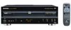
DV-505 DV-S9 DVD LD PLAYER DVL-909 SERVICE GUIDE ORDER NO. RRV1896 CONTENTS 1. CIRCUIT DESCRIPTION 2 2. CIRCUIT DESCRIPTIONS FOR DV-S9 AND DV-09 10 3. TEST MODE 13 4. IC INFORMATION 22 5. FL INFORMATION 47 PIONEER ELECTRONIC CORPORATION 4-1, Meguro 1-Chome, Meguro-ku, Tokyo 153-8654, Japan - Pioneer DVL-909 | Service Guide - Page 2
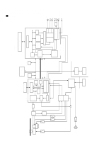
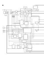
DV-505, DVL-909, DV-S9 1. CIRCUIT DESCRIPTION 1.1 OVERALL BLOCK DIAGRAM DV-505 2 Spindle TA Motor FA Slider Loading Motor HA OEIC IC301 TLC5540INS A/D TE GEN IC701 PD4833A LSI-11 IC702 HM514800CJ-7 4M bit DRAM VBR Buffer Sync Demod Spindle control DRAM I/F (bus arbitor) ECC & ID Reg. CPU - Pioneer DVL-909 | Service Guide - Page 3
Sub- GUI Video picture Decoder Decoder MIX AV Sync controller AC3/MPEG1 Audio Decoder DVD/V-CD IC801 AV Decoder MB86371 (MPEG2 Decoder) S/PDIF Servo DSP Mechanism IC501 Control PD4889A CPU 8 (OPTICAL) (COAXIAL) Digital Out DV-505, DVL-909, DV-S9 Loading Motor Mechanism sense SW DV - Pioneer DVL-909 | Service Guide - Page 4
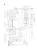
DV-505, DVL-909, DV-S9 DVL-909 SPDL Motor TA FA Slider For CLD TA FA Slider For DVD HA OEIC TE GEN IC701 PD4833A LSI-11 4Mbit DRAM VBR Buffer IC702 HM514800CJ-7 DRAM I/F (Bus Arbiter) IC601 PD3381A System CPU (32bit RISC) IC603 FLASH ROM IC602 IC604 GUI ROM RAM Sync A/D Demod CPU - Pioneer DVL-909 | Service Guide - Page 5
-505, DVL-909, DV-S9 IC802 MB811171622A -100FN 16Mbit SDRAM CODE Buffer (Video, Audio, Sub-picture,GUI) IC 801 MB86371 CPU I/F Memory Controller System Decoder (DMUX) MPEG 2 Sub Video Picture GUI Decoder Decoder 27M AV Sync Controller 36M DVD/V-CD AV Decoder MIX Copy Gurd NTSC /PAL - Pioneer DVL-909 | Service Guide - Page 6
DV-505, DVL-909, DV-S9 1.2 EXPLANATION OF EACH MOVEMENT 1.2.1 Sequence Up to Playback DVD SETUP RF AGC ON LD ON Sweep UP → Down Focus Lock . When the servo is turned on, the level of PH (the envelope of the bright side of RF) increases, and DRF becomes H. The kick-brake pulses, such as those for - Pioneer DVL-909 | Service Guide - Page 7
DVL-909 DIGITAL ADDRESS SERVO IC 46 & BUS IC501 MECH. CONTROL TDO: In addition to the servo output, the lowband components, such as the kick-brake for jump, are ERR signal is output from pin 48. For a DVD, the SPDL ERR signal is generated from the PWM signal output from LSI-ΙΙ. Upon receiving - Pioneer DVL-909 | Service Guide - Page 8
DV-505, DVL-909, DV-S9 1.2.5 Disc Determination Determination is achieved by checking the sine wave by sweeping the lens with the OE IC gain at L and the FSC - Pioneer DVL-909 | Service Guide - Page 9
Control (DVL-909) FLPB, KEYB DVD MAIN 13 16 102,107,108,111 IC101 PD4890A Mode Control (FL Cont.) 22 21 SI1,SO1 SCK1,XRDY KEY Remote Sensor IC601 PD3381A System Cont. IC604 Work RAM IC603 FLASH ROM IC602 GUI 4M ROM DATA,ADDRESS MAIN BUS MAD0-MAD7 IC801 MB86371 AV-Dec. POWER LD/DVD - Pioneer DVL-909 | Service Guide - Page 10
here is a DVD digital component signal (4:2:2), while it is an LD digital composite signal in conventional laser-disc players. DATA (3) Y/C-timing the system control computer by serial transmission, data for one frame are frozen, and the frozen picture is output. This function is specific to the - Pioneer DVL-909 | Service Guide - Page 11
the DVD MAIN Assy players. The register port output in serial communication that the PD0259A receives from the system-control computer is used as the control signal for analog noise reduction. After analog noise reduction, a CVBS signal is generated video signals. DV-505, DVL-909, DV-S9 4M DRAM µ- - Pioneer DVL-909 | Service Guide - Page 12
DV-505, DVL-909, DV-S9 to the AUDIO Assy. The switching control line (DAC MODE) is supplied from the DVD MAIN Assy. The master clock (MCK) is generated by a crystal on the AUDIO for 24 bits. Hi Bit IC101 Legato S IC111 Mode) When the user selects DAC mode, the DAC MODE port is set to H and VCO - Pioneer DVL-909 | Service Guide - Page 13
DV-505, DVL-909, DV-S9 3. TEST MODE 3.1 HOW TO ENTER THE TEST MODE There is the three following methods in an enters of the test mode. 1. Short-circuit the terminals (TP6006 and TP6007) for test mode entry at the side of the system control IC (IC601) of DVDM ASSY, and turn the power on. 2. Input [ - Pioneer DVL-909 | Service Guide - Page 14
, DVL-909, DV-S9 (11) Tracking Close 1. Press [STEP RVS] (50) key of the remote control unit in the play condition. 2. Switch the open/close by pressing [PLAY] key of the remote control unit or the player during the play (CD only). (12) Slider In 1. Press [SCAN RVS] (11) key of the remote control - Pioneer DVL-909 | Service Guide - Page 15
DV-505, DVL-909, DV-S9 3.4 EXPANSION FUNCTION 1 Set the reception mode of expansion function by pressing [TEST] (5E) key of the test mode remote control unit, then expansion function is able to execute by pressing the key of [0] to [9]. Indication for the most significant digit becomes "T" during - Pioneer DVL-909 | Service Guide - Page 16
Key Name of Remote Control Unit PGM+1 to 6 CLEAR +10 CHAP/TIME SIDE A SIDE B STEP FWD STEP REV SCAN REV Shuttle REV SCAN REV Shuttle REV SCAN FWD Shuttle FWD SCAN FWD Shuttle FWD SKIP REV SKIP FWD SPEED DOWN SPEED UP SKIP REV SKIP FWD SKIP FWD SKIP REV TEST + 1 TEST + 2 TEST + 3 MULTI FWD MULTI - Pioneer DVL-909 | Service Guide - Page 17
ATB : ON/OFF information display and AGC manual establishment display deleted with the second generation. FL controller version GUI-ROM number Part No. of flash ROM and system controller Part No. of DVD mechanism controller Part No. of CLD mechanism controller Second screen display (at lower right - Pioneer DVL-909 | Service Guide - Page 18
) RL : /RL, WY: /WY, RD: /RD. ∗ Furthermore DVL-91/KU/CA indicates as L91/K. (17) Region setting of the player [REG:∗] Setting value [1] to [6] (18) Version of the flash ROM [V:∗.∗∗] (19) Revision of the system controller [S Revision number of the external ROM part (flash ROM) of the system - Pioneer DVL-909 | Service Guide - Page 19
-505, DVL-909, DV-S9 (20) Revision of the DVD mechanism controller [M Revision number of the external ROM part (flash ROM) of the DVD mechanism controller Revision of the internal ROM (core part) of the DVD mechanism controller (21) Revision of the CLD mechanism controller - Pioneer DVL-909 | Service Guide - Page 20
and "compatibles" represents DVD-LD compatible models, such as the DVL-909. (1) Closes the tray. generated. The types of error that triggers the backup process for disc distinction are discussed in the next section. Using the Function in Test Mode This function is not assigned to any remote control - Pioneer DVL-909 | Service Guide - Page 21
DVL-909 DVD/LDcompatible models. As with the code misread errors below, they can also be generated reflection), or a pickup problem (dirty lens, etc.), remote control in Test mode is greater than 5, the cause may be (1). If the value is less then 3, the cause may be (2). (∗) With a specific - Pioneer DVL-909 | Service Guide - Page 22
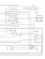
DV-505, DVL-909, DV-S9 4. IC INFORMATION • The information shown in the list is basic SRM2B256SLMX70, VYW1536, PD3381A, MB86371, MB811171622A-100FN, CY2081SL-611, PD2058A PD4890A (FLKB ASSY : IC101) • Mode Control IC • Block Diagram TO0/P30 43 TI0/INTP0/P00 47 TO1/P31 42 TI1/P33 40 TO2/P32 41 TI2 - Pioneer DVL-909 | Service Guide - Page 23
18 P74 (NC) (DV-505) SIDE A LED (DVL-909) 19 P73 (NC) (DV-505) SIDE B LED (DVL-909) 20 AVss Vss 21 P17 POWER ON 22 P16 RESET OUT 23 H : ON − Power supply pin O Not used O DVD lamp ON/OFF H : ON O Communication handshake line with the system controller L :Permit the communication - Pioneer DVL-909 | Service Guide - Page 24
P03 ON POWER 46 P01 LT 47 P00 SEL IR 48 IC IC 49 P72 (NC) 50 P71 FL OFF LED (DV-505) (NC) (DVL-909) 51 P70 the STBY/POWER ON at rising edge the FL controller L : STBY I Communication handshake line with the system controller H : Permit the communication I Remote control signal input - Pioneer DVL-909 | Service Guide - Page 25
ASSY : IC101)(DVL-909 ONLY) • Mechanism Control IC • CNVSS 28 XRESET 29 XIN 30 XOUT I/O Function I Power supply pin Apply 5V ± 10% O DSP read LD/CDV "L"= During vertical sync. I Ground for A/D conversion I Reset signal input "L"= Reset "H"= Release reset Control with the DVD mechanism control - Pioneer DVL-909 | Service Guide - Page 26
DV-505, DVL-909, DV-S9 No. Pin Name 31 PHAI PAL O Noise reduction control output by VDEM "L"= Normal "H"= Not NR I Disc present/absent detecting signal input by the tilt sum in the DVD P.U. mode "H"= Absent "L"= Present DEFECT input at LD P.U. I Turn switch input "H"= Side A / turn "L"= Side - Pioneer DVL-909 | Service Guide - Page 27
DV-505, DVL-909, DV-S9 LA9700M (DVDM PD 10p 15k 60k - + 60k 15k 10p REF 26p 40k 60k 40k - + 40k 40k 60k 26p REF APC LDS 12 + - + + - 1k 48 BPI1 REF VCC 47 VCC - 46 BPO1 45 EQB 3k 44 BPO2 28 29 30 31 32 QPH/BH DVD/CD DPD/TE CPOF TEBAL SGC TES TESI RREC TE TLP CP TEO TE- FE - Pioneer DVL-909 | Service Guide - Page 28
DV-505, DVL-909, DV-S9 BA6195FP (DVDM ASSY : IC161) • Spindle Driver • Block 16 N.C. 17 VCC 18 N.C. 19 GND 20 GND 21 N.C. 22 MUTE 23 N.C. 24 OPIN + Function Non Connection Power supply pin Non Connection Sub-strait GND pin Non Connection Mute pin Non Connection OP amp. non-inverting input pin 25 - Pioneer DVL-909 | Service Guide - Page 29
DV-505, DVL-909, DV-S9 LC78650E-P (DVDM ASSY : IC201)(DVL-909 only) • Servo DSP LSI • Block Diagram BUSYB 75 LASER 54 PP0-4 96-100 RESB 59 FG Counter SLC CD-PLL DVD-PLL Clock Generator Command Interface LCD Driver CLV Frame Synchronous Detection, Protection, Insertion EFM Demodulation Sub Code - Pioneer DVL-909 | Service Guide - Page 30
DV-505, DVL-909, DV-S9 • Pin 49 FDO 50 TDO I/O Function I/O General-purpose port input/output / DVD sync. signal input O Output the state that cut and out a pump for SLC − Control output 1 for SLC − Control output 2 for SLC I Test input 1 I EFM/EFM + input − 5V power supply of A/D and - Pioneer DVL-909 | Service Guide - Page 31
DVL-909 Test input 4 O Track detection signal output O For laser ON/OFF control O Disc discrimination result output O Pickup liquid shutter control of PLL constant current charge pump for EFM/EFM + playback − PLL 5V power supply for EFM/EFM + playback − VCO oscillation range setting of PLL for - Pioneer DVL-909 | Service Guide - Page 32
controller "L" (DVL-909 only) 6 P35/PCL 7 XTOFF − Not used (pull down) I/O High impedance (input) at DEFECT ON "L" output at DEFECT OFF 38 XABUSY 39 XIRQ2 INT DSP auto sequence busy input "L" INT LSI-11 interrupt input "L" 8 XCBUSY I DVD command reception is possible "L" 40 VDD − Power - Pioneer DVL-909 | Service Guide - Page 33
DVL-909, DV-S9 SRM2B256SLMX70 (DVDM ASSY : IC502) • 256 K SRAM (For Mechanism Control IC) • Block Diagram A0 10 A1 9 A2 8 A3 7 A4 6 A5 5 A6 4 A7 3 A8 25 A9 24 A10 21 A11 23 A12 2 A13 26 A14 1 Address Buffer 9 Line 512 Decoder 6 Row 64 Decoder CS 20 CS Control Power supply (2.7 to 5.5V) 33 - Pioneer DVL-909 | Service Guide - Page 34
DVL-909 only) • Flash ROM • Block Diagram WE 43 BYTE 33 RESET 44 CE 12 OE 14 RY/BY 1 RY/BY BUFFER RY/BY ERASE CIRCUIT DQ0-DQ15 15-22, 24-31 INPUT/OUTPUT BUFFER CONTROL 38 A12 39 A11 40 A10 41 A9 42 A8 43 WE 44 RESET Function Power supply (+5.0V ± 10% or ± 5%) Data input / output Data input/ - Pioneer DVL-909 | Service Guide - Page 35
(DVDM ASSY : IC601) • System Control CPU • Block Diagram DV-505, DVL-909, DV-S9 PA15/IRQ3/DREQ1 PA14/IRQ2 INTERRUPT USER BREAK CONTROLLER CONTROLLER DIRECT MEMORY ACCESS CONTROLLER BUS STATE CONTROLLER SERIAL COMMUNICATION INTERFACE (×2CHANNEL) PROGRAMABLE TIMING PATTERN CONTROLLER 16BIT - Pioneer DVL-909 | Service Guide - Page 36
DV-505, DVL-909, DV-S9 • Pin Function No. Pin Name 1 PB14/TP14/IRQ6 2 PB15/TP15/IRQ7 3 Interruption request I Ground I/O 16 bit bilateral data bus I Ground I/O 16 bit bilateral data bus I Power supply I/O 16 bit bilateral data bus I Ground O Address bus output (upper byte strobe signal) O - Pioneer DVL-909 | Service Guide - Page 37
, DVL-909, DV I/O 16 bit input/output (port A) / Data bus parity on the lower side / ITU input capture input/ITU output compare output (channel 1) I/O 16 bit A) / Interruption request / DMA transfer request (channel 1) I Power supply O System clock output I Ground I Crystal oscillator input - Pioneer DVL-909 | Service Guide - Page 38
DV-505, DVL-909, DV-S9 No. Pin Name 85 AVCC 86 AVREF 87 PC0/ PB10/TP10/RXD1 110 PB11/TP11/TXD1 111 PB12/TP12/IRQ4/SCK0 112 PB13/TP13/IRQ5/SCK1 I/O I Analog power supply I Analog reference power supply Function I 8 bit input (port C) / Analog signal input I Analog Ground I 8 bit input - Pioneer DVL-909 | Service Guide - Page 39
, DVL-909, DV-S9 16Mbit SDRAM CPU Interface System Decoder Block Internal Bus Memory Controller Block Reset Signal Clock Signal 27MHz LPF VCO Sync. Control Block Video Decoder Block Control Block Starting Signal Reset Signal Whole Control Block Audio Decoder Block System Clock Generation - Pioneer DVL-909 | Service Guide - Page 40
RBSEL 13 XHS O Digital component signal output Digital Y signal output (9-bit) − 3.3V power supply O Digital component signal output (LSB) Digital (LD mode) 43 N.C. O KEY signal for LD and OSD overlay (LD mode) 44 VSSA1 O Phase comparison result output signal of horizontal sync. (LD mode - Pioneer DVL-909 | Service Guide - Page 41
DV-505, DVL-909, DV-S9 No. Pin Name 53 DAIIN 54 CDDATA 55 CDLR 56 address bus signal 95 HADRS7 96 VSS 97 VDD 98 HADRS6 99 HADRS5 100 HADRS4 101 HADRS3 − GND − 3.3V power supply CPU address bus signal I 102 HADRS2 CPU address bus signal (LSB) 103 HDATA15 104 HDATA14 105 HDATA13 106 HDATA12 - Pioneer DVL-909 | Service Guide - Page 42
DV-505, DVL-909, DV-S9 No. Pin Name I/O Function 131 VDD − 3.3V power supply 132 XINT0 O Interrupt request signal to System clock output 200 VSSA(VCO) − GND (for VCO only) 201 VDDA(VCO) − 3.3V power supply (for VCO only) 202 ILPF O PLL block inverter output for audio 203 MLPF I PLL block - Pioneer DVL-909 | Service Guide - Page 43
DVL-909, DV-S9 MB811171622A-100FN (DVDM ASSY : IC802) • Code Buffer (16M bit SDRAM) • Block Diagram CLK 35 CKE 34 CS 18 RAS 17 CAS 16 WE 15 Clock Buffer Command Decoder To Blocks Control Address input Row : A0 to A10 , Column : A0 to A7 Power supply (+ 3.3V) 1,7,13,25,38,44 VCC/VCCQ 4,10,26, - Pioneer DVL-909 | Service Guide - Page 44
DV-505, DVL-909, DV-S9 CY2081SL-611 (DVDM ASSY : IC813) • Clock Generate IC • Block Diagram XTALIN 3 XTALOUT 4 Refference Oscillator GND 2 VDD 7 OE/ Configurable clock output Voltage supply Output control pin Either active-High output enable, active-Low power down, CLKA frequency select, or - Pioneer DVL-909 | Service Guide - Page 45
: IC901 )(DV-505 and DVL-909 only) • Digital Signal Processor For Audio • Block Diagram RST TES0 TES2 TPS0 TPS16 VDDR VSSR VDD VSS 45 42-44 1-3,6-11, 53-60 Data RAM 128w×24b Coefficient RAM 320w×16b Coefficient ROM 256w×16b Offset RAM 64w×16b Delay RAM Address Generating Circuit 13 12 4,31 - Pioneer DVL-909 | Service Guide - Page 46
DVL-909 data length is able to select the 24-bit or 16-bit by controlling the microprocessor. O LR clock output pin (1 fs) O Word clock output low-pass filter I Amp. input pin for low-pass filter − Analog power supply pin I Test pin Normally, use for "H" or open. I Reset signal input pin I - Pioneer DVL-909 | Service Guide - Page 47
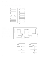
-S9 5. FL INFORMATION VAW1046 (FLKB ASSY : V101)(DV-505 and DVL-909 only) • FL DISPLAY 1 34 96kHz GUI P1 TITLE PB G1 ANGLE LAST MEMO CONDITION DOLBY CHP / TRK P6 REMAIN TOTAL DIGITAL G2 G3 G4 G5
-
 1
1 -
 2
2 -
 3
3 -
 4
4 -
 5
5 -
 6
6 -
 7
7 -
8
-
9
-
10
-
11
-
12
-
13
-
14
-
15
-
16
-
17
-
18
-
19
-
20
-
21
-
22
-
23
-
24
-
25
-
26
-
27
-
28
-
29
-
30
-
31
-
32
-
33
-
34
-
35
-
36
-
37
-
38
-
39
-
40
-
41
-
42
-
43
-
44
-
45
-
46
-
47
 |
 |
ORDER NO.
RRV1896
T - IZM
APR. 1998 Printed
in Japan
PIONEER ELECTRONIC CORPORATION
4-1, Meguro 1-Chome, Meguro-ku, Tokyo 153-8654, Japan
PIONEER ELECTRONICS SERVICE, INC.
P.O. Box 1760, Long Beach, CA 90801-1760, U.S.A.
PIONEER ELECTRONIC (EUROPE) N.V.
Haven 1087, Keetberglaan 1, 9120 Melsele, Belgium
PIONEER ELECTRONICS ASIACENTRE PTE. LTD.
501 Orchard Road, #10-00 Lane Crawford Place, Singapore 0923
PIONEER ELECTRONIC CORPORATION 1998
c
1. CIRCUIT DESCRIPTION
......................................
2
2. CIRCUIT DESCRIPTIONS
FOR DV-S9 AND DV-09
...............................
10
3. TEST MODE
.......................................................
13
4. IC INFORMATION
..............................................
22
5. FL INFORMATION
..............................................
47
CONTENTS
DV-505
DVD
PLAYER
DV-S9
DVD LD
PLAYER
DVL-909
SERVICE GUIDE