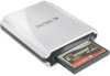
SanDisk SDCFRX4-2048-901 Product Manual
SanDisk SDCFRX4-2048-901 - 2 GB Extreme IV CompactFlash Card Manual
 |
UPC - 619659028954
View all SanDisk SDCFRX4-2048-901 manuals
Add to My Manuals
Save this manual to your list of manuals |
SanDisk SDCFRX4-2048-901 manual content summary:
- SanDisk SDCFRX4-2048-901 | Product Manual - Page 1
SanDisk CompactFlash Memory Card OEM Product Manual Version 12.0 Document No. 20-10-00038 02/2007 SanDisk Corporation Corporate Headquarters 601 McCarthy Boulevard Milpitas, CA 95035 (408) 801-1000 Phone (408) 801-8657 Fax www.sandisk.com - SanDisk SDCFRX4-2048-901 | Product Manual - Page 2
- SanDisk SDCFRX4-2048-901 | Product Manual - Page 3
Card OEM Product Manual SanDisk® Corporation general policy does not recommend the use of its products in life support applications where in a failure or malfunction of the product may directly threaten life or injury. Per SanDisk Terms and Conditions of Sale, the user of SanDisk products in - SanDisk SDCFRX4-2048-901 | Product Manual - Page 4
SanDisk CompactFlash Card OEM Product Manual -This page intentionally left blank- 02/07, Rev. 12.0 ii © 2007 SanDisk Corporation - SanDisk SDCFRX4-2048-901 | Product Manual - Page 5
Configuration 3-20 I/O Transfer Function 3-25 True IDE Mode I/O Transfer Function 3-26 ATA Register Set and Protocol 4-1 I/O Primary and Secondary Address Configurations 4-1 Contiguous I/O Mapped Addressing 4-2 © 2007 SanDisk Corporation i Rev. 12.0, 02/07 - SanDisk SDCFRX4-2048-901 | Product Manual - Page 6
Table of Contents CHAPTER 5 CHAPTER 6 APPENDIX A APPENDIX B APPENDIX C SanDisk CompactFlash Card OEM Product Manual Memory Mapped Addressing 4-3 True IDE Mode Addressing 4-4 ATA Registers 4-4 ATA Command Description 5-1 ATA Command Set 5-1 Error Posting 5-29 CIS Description 6-1 Ordering - SanDisk SDCFRX4-2048-901 | Product Manual - Page 7
is JEIDA.) The CompactFlash Memory Card Series also supports a True IDE Mode that is electrically compatible CompactFlash Memory cards use SanDisk Flash memory, which was designed by SanDisk specifically for use in . The host addresses the card in 512 byte sectors. Each sector is protected by a - SanDisk SDCFRX4-2048-901 | Product Manual - Page 8
• +5 Volts or +3.3 Volts operation • Automatic error correction and retry capabilities • Supports power down commands and sleep modes • Non-volatile storage (no battery required) • specifications are not covered in this manual. 1.4 CompactFlash Standard SanDisk CompactFlash Memory cards are fully - SanDisk SDCFRX4-2048-901 | Product Manual - Page 9
CompactFlash Card OEM Product Manual Introduction 1.5 PCMCIA Standard SanDisk CompactFlash Memory cards are fully electrically compatible with the PCMCIA specifications listed below: • PCMCIA PC Card Standard, 7.0, February 1999 • PCMCIA PC Card ATA Specification, 7.0, February - SanDisk SDCFRX4-2048-901 | Product Manual - Page 10
Introduction SanDisk CompactFlash Card OEM Product Manual 1.7.1 Technology Independence The 512-byte sector size of the CompactFlash life expectancy. 1.7.4 Using Erase Sector and Write Commands SanDisk CompactFlash Memory cards support the CF ERASE SECTOR and WRITE WITHOUT ERASE commands. - SanDisk SDCFRX4-2048-901 | Product Manual - Page 11
Card OEM Product Manual Introduction 1.7.5 Automatic Sleep Mode A unique feature of the SanDisk CompactFlash Memory Card is overhead but this must be done only for the SanDisk products as other ATA products may not support this feature. 1.7.6 Dynamic Adjustment of Performance vs. - SanDisk SDCFRX4-2048-901 | Product Manual - Page 12
Introduction SanDisk CompactFlash Card OEM Product Manual -This page intentionally left blank- 02/07, Rev. 12.0 1-6 © 2007 SanDisk Corporation - SanDisk SDCFRX4-2048-901 | Product Manual - Page 13
. maximum 80,000 ft. maximum 2.2 System Power Requirements All values quoted in Table 2-2 are typical at 25° C and nominal supply voltage unless otherwise stated. © 2007 SanDisk Corporation 2-1 Rev. 12.0, 02/07 - SanDisk SDCFRX4-2048-901 | Product Manual - Page 14
Product Specifications SanDisk CompactFlash Card OEM Product Manual Sleep mode currently is specified under mA Read/Write Peak 100 mA Memory Subsystema CompactFlash Extreme III Memory Card Sleep Up to 512 MB 300 µ 512 MB to 1.5 GB 600 µ Over 1.5 GB 1 mA Read 75 mA Write 75 mA Read/ - SanDisk SDCFRX4-2048-901 | Product Manual - Page 15
SanDisk CompactFlash Card OEM Product Manual Product Specifications 2.3 System Performance All performance timings ms maximum 20 ms maximum 50 ms typical; 400 ms maximum Programmable 20.0 MB/sec burst 16.0 MB/sec burst Controller Overhead Command to DRQ 50 ms maximum CompactFlash Extreme III - SanDisk SDCFRX4-2048-901 | Product Manual - Page 16
Product Specifications SanDisk CompactFlash Card OEM Product Manual 2.4 System Reliability Table 2-4 Reliability MTBF (@ 25 C) Preventative Maintenance Data Reliability >1,000,000 685 ± .004 in) 3.3 mm ± 0.10 mm (.130 ± .004 in) (Excluding Lip) 02/07, Rev. 12.0 2-4 © 2007 SanDisk Corporation - SanDisk SDCFRX4-2048-901 | Product Manual - Page 17
SanDisk CompactFlash Card OEM Product Manual Figure 2-1 CompactFlash Memory Card Dimensions Product Specifications © 2007 SanDisk Corporation 2-5 Rev. 12.0, 02/07 - SanDisk SDCFRX4-2048-901 | Product Manual - Page 18
Product Specifications SanDisk CompactFlash Card OEM Product Manual -This page intentionally left blank- 02/07, Rev. 12.0 2-6 © 2007 SanDisk Corporation - SanDisk SDCFRX4-2048-901 | Product Manual - Page 19
CHAPTER 3 Interface Description 3.1 Physical Description The host connects to SanDisk CompactFlash Memory cards using a standard 50-pin connector consisting of two rows of 25 female contacts OT1 I3U I1U,OT1 I1U,OT1 I1Z,OZ3 I1Z,OZ3 I1Z,OZ3 Ground © 2007 SanDisk Corporation 3-1 Rev. 12.0, 02/07 - SanDisk SDCFRX4-2048-901 | Product Manual - Page 20
Interface Description SanDisk CompactFlash Card OEM Product Manual PC Card I/O Pin Assignments are contained in Table 3-2. Table 3-2 Pin No. 1 2 3 4 5 6 7 8 9 10 11 12 I/O I/O I O I/O Type Ground I1Z,OZ3 I1Z,OZ3 I1Z,OZ3 I1Z,OZ3 I1Z,OZ3 I3Z Ground 02/07, Rev. 12.0 3-2 © 2007 SanDisk Corporation - SanDisk SDCFRX4-2048-901 | Product Manual - Page 21
SanDisk CompactFlash Card OEM Product Manual Interface Description Table 3-3 True IDE Mode Pin Assignments Pin The CompactFlash Memory Card Series is optimized for operation with hosts, which support the PCMCIA I/O interface standard conforming to the PC Card ATA specification. However - SanDisk SDCFRX4-2048-901 | Product Manual - Page 22
Product Manual The SanDisk CompactFlash the card, memorymapped port address registers within the card, a byte in the card's information structure and its configuration control and a high state in I/O Mode since this product does not support the audio function. -DASP (True IDE Mode) In the True - SanDisk SDCFRX4-2048-901 | Product Manual - Page 23
SanDisk CompactFlash Card OEM Product Manual Interface Description Table 3-4 Signal Description Signal status information between the host and the controller. D00 is the LSB of the Even Byte of the word. D08 is the LSB of the Odd Byte of the word. D15-D00 (True IDE Mode) In True IDE Mode, all - SanDisk SDCFRX4-2048-901 | Product Manual - Page 24
Interface Description SanDisk CompactFlash Card OEM Product Manual Table 3-4 Signal Description Signal Name Dir. Pin -IOWR (PC Card I/O Mode) (True IDE Mode) -OE I 9 (PC Card Memory low) during I/O cycles when the I/O address is on the bus. 02/07, Rev. 12.0 3-6 © 2007 SanDisk Corporation - SanDisk SDCFRX4-2048-901 | Product Manual - Page 25
SanDisk CompactFlash Card OEM Product Manual Interface Description Table 3-4 Signal Description Signal Name Dir. Pin -DMACK (True IDE Mode) RESET I (PC Card Memory Mode) (PC Card I/O Mode) -RESET (True IDE Mode) - SanDisk SDCFRX4-2048-901 | Product Manual - Page 26
Interface Description SanDisk CompactFlash Card OEM Product Manual Table 3-4 Signal Description Signal Name Dir. Pin - 16 Bit Port (-IOIS16) function. A low signal indicates that a 16-bit or odd-byte only operation can be performed at the addressed port. This output signal is asserted low - SanDisk SDCFRX4-2048-901 | Product Manual - Page 27
SanDisk CompactFlash Card OEM Product Manual Interface Description Table 3-6 defines the input characteristics of the parameters in Table 3-5. Table 3-6 Input -0.8V Gnd +0.4V X Tri-State Leakage Current loz Vol = Gnd -10 Voh = VCC 10 uA © 2007 SanDisk Corporation 3-9 Rev. 12.0, 02/07 - SanDisk SDCFRX4-2048-901 | Product Manual - Page 28
Interface Description SanDisk CompactFlash Card OEM Product Manual 3.3.3 Power Up/Power Down Timing The and falling time must be met by this specification. Figure 3-1 Power Up/Power Down Timing for Systems supporting RESET tpr tSU(VCC) VCC Min. VIH 2V Hi-z tW(Reset) VCC -CE1, -CE2 tSU( - SanDisk SDCFRX4-2048-901 | Product Manual - Page 29
SanDisk CompactFlash Card OEM Product Manual Interface Description Figure 3-2 Power Up/Power Down Timing for Systems not supporting RESET ta (CE) ta (OE) tdis (OE) tdis (CE) ten (CE) ten (OE) tv (A) tsu (A) IEEE Symbol tAVAV tAVQV tELQV tGLQV tGHQZ tEHQZ tELQNZ tGLQNZ tAXQX tAVGL 100 ns Min. - SanDisk SDCFRX4-2048-901 | Product Manual - Page 30
Interface Description SanDisk CompactFlash Card OEM Product Manual Table 3-10 Common Memory Read Timing Specification Speed system driver/receiver to the card must be accounted for by the system NOTE: SanDisk CompactFlash Memory cards do not assert the -WAIT signal. Table 3-11 Common and - SanDisk SDCFRX4-2048-901 | Product Manual - Page 31
Manual Interface Description 3.3.6 Attribute Memory Read Timing Specification Table 3-12 contains common memory write timing specifications for all types of memory. NOTE: SanDisk tc (R) ta (A) ta (CE) ta (OE) tdis (OE) ten (OE) tv (A) tsu (A) th (A) tsu(CE) th (CE) IEEE Symbol tAVAV tAVQV tELQV - SanDisk SDCFRX4-2048-901 | Product Manual - Page 32
Interface Description SanDisk CompactFlash Card OEM Product Manual Figure 3-4 Common and Attribute Memory Write Timing Diagram NOTE 1: NOTE 2: but restrictions on -OE from previous figures apply. SanDisk CompactFlash Memory Cards do not assert the -WAIT signal. 02/07, Rev. 12.0 3-14 © 2007 - SanDisk SDCFRX4-2048-901 | Product Manual - Page 33
SanDisk CompactFlash Card OEM Product Manual 3.3.8 I/O Read (Input) Timing Specification Figure 3-5 I/O Read Timing Diagram to the host system. Table 3-13 contains the read input timing specifications. NOTE: SanDisk CompactFlash Memory cards do ont assert a -WAIT signal. Table 3-13 I/O Read - SanDisk SDCFRX4-2048-901 | Product Manual - Page 34
Interface Description SanDisk CompactFlash Card OEM Product Manual Table 3-13 I/O Read (Input) Timing Specification Item -IOIS16 Delay falling from Address -IOIS16 Delay rising from provided by the host system to the CompactFlash Memory Card. 02/07, Rev. 12.0 3-16 © 2007 SanDisk Corporation - SanDisk SDCFRX4-2048-901 | Product Manual - Page 35
SanDisk CompactFlash Card OEM Product Manual Interface Description Table 3-14 contains the specification and measured at the connector of the selected device. Transfer Timing. The minimum cycle time supported by devices in PIO Mode 3, 4 and Multiword DMA Mode 1, 2 respectively will always - SanDisk SDCFRX4-2048-901 | Product Manual - Page 36
Interface Description SanDisk CompactFlash Card OEM Product Manual Figure 3-7 Register Transfer to/from Device the value reported in the devices IDENTIFY DEVICE data. A device imple mentation shall support any legal host implementation. b. This parameter specifies the time from the negation edge - SanDisk SDCFRX4-2048-901 | Product Manual - Page 37
SanDisk CompactFlash Card OEM Product Manual Interface Description • PIO Data Transfers Figure 3-8 defines the relationships between the interface signals for Device address consists of signals -CS0, -CS1 and -DA(2:0). Data consists of DD(15:0). © 2007 SanDisk Corporation 3-19 Rev. 12.0, 02/07 - SanDisk SDCFRX4-2048-901 | Product Manual - Page 38
Card OEM Product Manual The PIO data transfer parameters are defined in Table 3-16. NOTE: SanDisk CompactFlash Memory value reported in the devices IDENTIFY DEVICE data. A device imple mentation shall support any legal host implementation. b. This parameter specifies the time from the negation - SanDisk SDCFRX4-2048-901 | Product Manual - Page 39
SanDisk CompactFlash Card OEM Product Manual Interface Description In addition, these registers provide a method for accessing status information about the card configuration register addresses. All other attribute memory locations are reserved. © 2007 SanDisk Corporation 3-21 Rev. 12.0, 02/07 - SanDisk SDCFRX4-2048-901 | Product Manual - Page 40
Interface Description SanDisk CompactFlash Card OEM Product Manual Decoding for Byte Read Word Access Configuration (16 bits) L L L H X L H Not Valid Even Byte Write Word Access Configuration (16 bits) L L L H X H L Don't Even Care Byte 02/07, Rev. 12.0 3-22 © 2007 SanDisk - SanDisk SDCFRX4-2048-901 | Product Manual - Page 41
SanDisk CompactFlash Card OEM Product Manual Interface Description 3.4.2 Configuration Option 0 Conf1 0 0 1 1 Conf0 0 1 0 1 Disk Card Mode Memory Mapped I/O Mapped; any 16-byte system decoded boundary I/O Mapped; 1F0-1F7/3F6-3F7 I/O Mapped; 170-177/376-377 3.4.3 Card Configuration and Status - SanDisk SDCFRX4-2048-901 | Product Manual - Page 42
Interface Description SanDisk CompactFlash Card OEM Product Manual Card Configuration and Status Register (con't) Bit . This signal remains true until the condition that caused the interrupt request has been serviced. If interrupts are disabled by the -IEN bit in the Device Control Register, - SanDisk SDCFRX4-2048-901 | Product Manual - Page 43
configuration is supported. The socket Byte Write Access (8 bits) -REG -CE2 -CE1 A0 -OE -WE D15-D8 X H H X X X High Z H H L L L H High Z H H L H L H High Z H H L L H L Don't Care H H L H H L Don't Care D7-D0 High Z Even Byte Odd Byte Even Byte Odd Byte © 2007 SanDisk - SanDisk SDCFRX4-2048-901 | Product Manual - Page 44
Description SanDisk CompactFlash Card OEM Product Manual Table 3-22 Common Memory Function Function Code -REG -CE2 -CE1 A0 -OE -WE Word Read Access H L L X L H (16 bits) Word Write Access (16 bits) H L L X H L Odd Byte Read Only H L H X L H (8 bits) Odd Byte Write - SanDisk SDCFRX4-2048-901 | Product Manual - Page 45
Protocol SanDisk CompactFlash Memory cards can be configured as a high performance I/O device through the following ways: • Standard PC-AT disk I/O address spaces 1F0h-1F7h, 3F6h-3F7h (primary); 170h-177h, 376h-377h (secondary) with IRQ 14 (or other available IRQ). • Any system decoded 16-byte - SanDisk SDCFRX4-2048-901 | Product Manual - Page 46
byte accesses to register 9 are not supported. However, repeated alternating byte accesses to registers 8 then 9 will access consecutive (even then odd) bytes from the data buffer. Byte accesses to register 9 access only the odd byte of the data. 02/07, Rev. 12.0 4-2 © 2007 SanDisk Corporation - SanDisk SDCFRX4-2048-901 | Product Manual - Page 47
SanDisk CompactFlash Card OEM Product Manual ATA Register Set and Protocol 4.3 Memory Mapped Addressing When CompactFlash Memory Card registers are accessed via memory references, they appear in the common memory space window: 0-2K bytes to memory block move instruction. Some PCMCIA socket - SanDisk SDCFRX4-2048-901 | Product Manual - Page 48
ATA Register Set and Protocol SanDisk CompactFlash Card OEM Product Manual 4.4 True IDE Mode Addressing When a CompactFlash Memory and Error/Feature Register rather than attempt to define general PCMCIA word and byte access modes and operations. Refer to the PCMCIA PC Card Standard Release 2.0 - SanDisk SDCFRX4-2048-901 | Product Manual - Page 49
SanDisk CompactFlash Card OEM Product Manual ATA Register Set and Protocol Table 4-6 Data Register Data Register Error/Feature Register Error/Feature Register CE2- CE1- ) for any CompactFlash Memory Card data access for the subsequent command. © 2007 SanDisk Corporation 4-5 Rev. 12.0, 02/07 - SanDisk SDCFRX4-2048-901 | Product Manual - Page 50
ATA Register Set and Protocol SanDisk CompactFlash Card OEM Product Manual 4.5.6 Cylinder Low (LBA 15-8) Register (Address-1F4[174]; Offset 4) This register contains the low order 8 head number. It is Bit 24 in the Logical Block Address mode. 02/07, Rev. 12.0 4-6 © 2007 SanDisk Corporation - SanDisk SDCFRX4-2048-901 | Product Manual - Page 51
SanDisk CompactFlash Card OEM Product Manual ATA Register Set and Protocol 4.5.9 Status & Alternate Status Registers (Address-1F7[177]&3F6[376]; Offsets 7 & Eh defined as follows: D7 D6 D5 D4 D3 D2 D1 D0 X X X X 1 SW Rst -IEn 0 © 2007 SanDisk Corporation 4-7 Rev. 12.0, 02/07 - SanDisk SDCFRX4-2048-901 | Product Manual - Page 52
ATA Register Set and Protocol SanDisk CompactFlash Card OEM Product Manual Device Control Register (con't) Bit Name Description D7 X Don't care. D6 X Don't care. D5 X Don't care. D4 D1 D0 X -WTG -HS3 -HS2 -HS1 -HS0 -nDS1 -nDS0 02/07, Rev. 12.0 4-8 © 2007 SanDisk Corporation - SanDisk SDCFRX4-2048-901 | Product Manual - Page 53
SanDisk CompactFlash Card OEM Product Manual ATA Register Set and Protocol Card (Drive) Address Register ( same addresses as the CompactFlash Memory Card. Following are some possible solutions to this problem for the PCMCIA implementation: 1. Locate the CompactFlash Memory Card at a non- - SanDisk SDCFRX4-2048-901 | Product Manual - Page 54
ATA Register Set and Protocol SanDisk CompactFlash Card OEM Product Manual -This page intentionally left blank- 02/07, Rev. 12.0 4-10 © 2007 SanDisk Corporation - SanDisk SDCFRX4-2048-901 | Product Manual - Page 55
D - 91h -Y - - Y - E4h - - - - D - C8 or C9 - YYYY Y C4h - YYYY Y 22h or 23h - - YY Y Y 20h or 21h - Y Y Y Y Y 40h or 41h - Y Y Y Y Y 1Xh - - - - D - 03h - - - - D - 7Xh - - YY Y Y EFh Y - - - D - © 2007 SanDisk Corporation 5-1 Rev. 12.0, 02/07 - SanDisk SDCFRX4-2048-901 | Product Manual - Page 56
ATA Command Description SanDisk CompactFlash Card OEM Product Manual Table 5-1 Primary and Secondary I/O Decoding Class 1 1 1 1 1 1 2 2 2 3 3 Cylinder Registers DH Card/Drive/Head Register LBA Logical Block Address Mode Supported Y The register contains a valid parameter for this command. For - SanDisk SDCFRX4-2048-901 | Product Manual - Page 57
SanDisk CompactFlash Card OEM Product Manual ATA Command Description If the card is in Idle mode, it sets BSY, sets the Sector Count device error Sector buffer error ECC circuitry error Controlling microprocessor error Slave failed (True IDE Mode) © 2007 SanDisk Corporation 5-3 Rev. 12.0, 02/07 - SanDisk SDCFRX4-2048-901 | Product Manual - Page 58
ATA Command Description SanDisk CompactFlash Card OEM Product Manual 5.1.3 Erase Sector(s)-C0H This command is no longer recommended. There is essentially no net gain in the use of the Erase Sectors Command and/or the Write Without Erase Commands. This command is supported to guarantee backward - SanDisk SDCFRX4-2048-901 | Product Manual - Page 59
SanDisk CompactFlash Card OEM Product Manual ATA Byte Order in Word Model number in ASCII (left justified) Big Endian Byte Order in Word Maximum No. of Sectors on Read/Write Multiple command Double-word not supported Capabilities: DMA Supported (bit 8), LBA supported (bit 9) Reserved © 2007 SanDisk - SanDisk SDCFRX4-2048-901 | Product Manual - Page 60
Description SanDisk CompactFlash Card OEM Product Manual Table 5-8 Identify Device Information Word Address 51 52 Default Value 0200h 0000h Total Bytes 2 mode Single word DMA data transfer cycle timing mode (not supported) Field validity Current number of cylinders Current number of heads - SanDisk SDCFRX4-2048-901 | Product Manual - Page 61
001Bh 0000h 0000h Total Bytes 2 2 22 140 Data Field Type Information CF Advanced True IDE Timing Mode Capability and Setting CF Advanced PCMCIA I/O and Memory Timing Mode Capability Reserved for assignment by the CFA Reserved a. Multiword DMA is supported by SanDisk PCMCIA. For all unsupported - SanDisk SDCFRX4-2048-901 | Product Manual - Page 62
SanDisk CompactFlash Card OEM Product Manual Word 21: Buffer Size. This field defines the buffer capacity of 2 sectors or 1 kilobyte of SRAM. Word 22: ECC Count. This field defines the number of ECC bytes DEVICE data. A device implementation shall support any legal host implementation. The IORD- - SanDisk SDCFRX4-2048-901 | Product Manual - Page 63
SanDisk CompactFlash Card OEM Product Manual other value returned by the CompactFlash Memory Card in the even byte is a 01H value, which indicates that 1 sector per interrupt nanoseconds, the minimum cycle time that the device can support when performing Multiword DMA transfers on a per word basis - SanDisk SDCFRX4-2048-901 | Product Manual - Page 64
ATA Command Description SanDisk CompactFlash Card OEM Product Manual Word 68: Minimum PIO Transfer Cycle Time With Flow Control. This field indicates in nanoseconds, the minimum cycle time the card supports while performing data transfers using flow control. Words 82-84: Features/Command Sets - SanDisk SDCFRX4-2048-901 | Product Manual - Page 65
SanDisk CompactFlash Card OEM Product Manual ATA Command Description Bits 0-13 of word 87 are 8 0 Service Interrupt not enabled 9 0 Device Reset command not supported 10 0 Host Protected Area feature set not supported 11 --- Obsolete 12 1 Write Buffer command supported by CF Card - SanDisk SDCFRX4-2048-901 | Product Manual - Page 66
ATA Command Description SanDisk CompactFlash Card OEM Product Manual • Bits 2-0: Advanced True IDE PIO Mode Support Indicates the maximum True IDE PIO mode supported by the card. Value 0 1 2 3-7 Maximum PIO Mode Timing Supported Specified in Word 64 PIO Mode 5 PIO Mode 6 Reserved • Bits 5-3: - SanDisk SDCFRX4-2048-901 | Product Manual - Page 67
SanDisk CompactFlash Card OEM Product Manual ATA Command Description Word 164: CF Advanced PCMCIA Bits 5-3: Maximum Memory Timing Mode Supported Indicates the Maximum Memory timing mode supported by the card. Value 0 1 2 3 4-7 Maximum Memory Timing Mode Supported 250 ns Cycle Memory Mode 120 ns - SanDisk SDCFRX4-2048-901 | Product Manual - Page 68
ATA Command Description SanDisk CompactFlash Card OEM Product Manual 5.1.7 Idle Immediate-95H, E1H This command causes Sector Count and the Card/Drive/Head registers are used by this command. NOTE: SanDisk recommends not using this command in any system because DOS determines the offset to the - SanDisk SDCFRX4-2048-901 | Product Manual - Page 69
SanDisk CompactFlash Card OEM Product Manual ATA Command Description 5.1.9 Read Buffer-E4H The Read Buffer command enables the host to 16) Cylinder Low (LBA 15-8) Sec Num (3) Sector Number (LBA 7-0) Sec Cnt (2) Sector Count Feature (1) X © 2007 SanDisk Corporation 5-15 Rev. 12.0, 02/07 - SanDisk SDCFRX4-2048-901 | Product Manual - Page 70
ATA Command Description SanDisk CompactFlash Card OEM Product Manual 5.1.11 Read Multiple-C4H The Read Multiple command performs similarly to the Read Sectors command. Interrupts are to stop after transfer of the block that contained the error. 02/07, Rev. 12.0 5-16 © 2007 SanDisk Corporation - SanDisk SDCFRX4-2048-901 | Product Manual - Page 71
SanDisk CompactFlash Card OEM Product Manual ATA Command Description 5.1.12 Read Long Sector-22H, 23H The Read Long command performs similarly to the Read Sector(s) command except that it returns 516 bytes of data instead of 512 bytes. During a Read Long command, the card does not check the ECC - SanDisk SDCFRX4-2048-901 | Product Manual - Page 72
ATA Command Description SanDisk CompactFlash Card OEM Product Manual When the requested sectors have been verified, the card (7) 03H C/D/H (6) 1 X 1 Drive X Cyl High (5) X Cyl Low (4) X Sec Num (3) X Sec Cnt (2) X Feature (1) X 02/07, Rev. 12.0 5-18 © 2007 SanDisk Corporation - SanDisk SDCFRX4-2048-901 | Product Manual - Page 73
SanDisk CompactFlash Card OEM Product Manual ATA Command Description Table 5-24 defines the valid extended error codes for the ) Cyl Low (4) Cylinder Low (LBA 15-8) Sec Num (3) Sector Number (LBA 7-0) Sec Cnt (2) X Feature (1) X © 2007 SanDisk Corporation 5-19 Rev. 12.0, 02/07 - SanDisk SDCFRX4-2048-901 | Product Manual - Page 74
ATA Command Description SanDisk CompactFlash Card OEM Product Manual 5.1.18 Set Features-EFH (1) Feature Table 5-27 defines all features that are supported. The 9AH feature is unique to CompactFlash Memory cards no impact on the CF Memory Card 4 bytes of data apply on Read/Write Long commands - SanDisk SDCFRX4-2048-901 | Product Manual - Page 75
SanDisk CompactFlash Card OEM Product Manual ATA Command Description A host can choose the transfer of sectors per block. The current version of the card supports only a block size of 1 sector per block. Future versions may support larger block sizes. Upon receipt of the command, the card - SanDisk SDCFRX4-2048-901 | Product Manual - Page 76
ATA Command Description SanDisk CompactFlash Card OEM Product Manual If the Sector Count Register contains a valid value and the block count is supported, the value is loaded for all subsequent Read Multiple and Write Multiple commands and execution of those commands is enabled. If a block count - SanDisk SDCFRX4-2048-901 | Product Manual - Page 77
SanDisk CompactFlash Card OEM Product Manual ATA Command Description 5.1.21 Standby-96H, X X 5.1.23 Translate Sector-87H When this command is issued, the controller responds with a 512-byte buffer of information on the desired cylinder, head and sector with the actual Logical Address. Table 5- - SanDisk SDCFRX4-2048-901 | Product Manual - Page 78
SanDisk CompactFlash Card OEM Product Manual Table 5-33 represents the information in the buffer. This command is unique to SanDisk desired. This command has the same protocol as the Write Sector(s) command and transfers 512 bytes. Table 5-35 Write Buffer Bit 7 6 5 4 3 2 1 0 Command (7) - SanDisk SDCFRX4-2048-901 | Product Manual - Page 79
SanDisk CompactFlash Card OEM Product Manual ATA Command Description 5.1.26 Write DMA Command-CAH, bytes instead of 512 bytes. Only single sector Write Long operations are supported. The transfer consists of 512 bytes of data transferred in word mode followed by 4 bytes of ECC transferred in byte - SanDisk SDCFRX4-2048-901 | Product Manual - Page 80
ATA Command Description SanDisk CompactFlash Card OEM Product Manual DRQ qualification of the transfer is required only at the start of the data block, not on each sector Count Register contains 6 and the address is that of the third sector. 02/07, Rev. 12.0 5-26 © 2007 SanDisk Corporation - SanDisk SDCFRX4-2048-901 | Product Manual - Page 81
CompactFlash Card OEM Product Manual ATA Command Description 5.1.29 Write Multiple without Erase-CDH SanDisk does not recommend the use of this command in new designs but it is supported as a normal Write Sectors command for backward compatibility reasons. Table 5-39 Write Multiple w/out - SanDisk SDCFRX4-2048-901 | Product Manual - Page 82
ATA Command Description SanDisk CompactFlash Card OEM Product Manual 5.1.31 Write Sector(s) without Erase-38H SanDisk does not recommend the use of this command in new designs but it is supported as a normal Write Sectors command for backward compatibility reasons. Table 5-41 Write Sector(s) w/ - SanDisk SDCFRX4-2048-901 | Product Manual - Page 83
SanDisk CompactFlash Card OEM Product Manual ATA Command Description 5.2 Error Posting - V V V V V V - V Invalid Command Code - - - V - V V V - V a. V = Valid on this command. b. CompactFlash products support multiword DMA. © 2007 SanDisk Corporation 5-29 Rev. 12.0, 02/07 - SanDisk SDCFRX4-2048-901 | Product Manual - Page 84
ATA Command Description SanDisk CompactFlash Card OEM Product Manual -This page intentionally left blank- 02/07, Rev. 12.0 5-30 © 2007 SanDisk Corporation - SanDisk SDCFRX4-2048-901 | Product Manual - Page 85
= 250 ns 2 kB of Address Space End of Devices JEDEC ID Common Memory Link is 2 bytes First byte of JEDEC ID for SanDisk PC Card ATA 12V Second Byte of JEDEC ID Manufacturer's ID Tuple Link is 4 bytes SanDisk JEDEC Manufacturer's ID Device ID, WPS, Speed Device Size End Marker Tuple Code Link Length - SanDisk SDCFRX4-2048-901 | Product Manual - Page 86
CIS Description SanDisk CompactFlash Card OEM Product Manual Table 6-1 Card Information Structure Attribute Offset Data 765 4 3 2 1 026h 00h High Byte of PCMCIA Manufacturer's Code 028h 01h 02Ah 04h 02Ch 15h 02Eh 17h 030h 04h 032h 01h 034h 53h 036h 61h 038h 6Eh 03Ah 44h - SanDisk SDCFRX4-2048-901 | Product Manual - Page 87
SanDisk CompactFlash Card OEM Product Manual CIS Description Table 6-1 Card present 1 0 0 0 TAR: Temp Bsy on AT Reset TPR: Temp Bsy on PCMCIA - Reset SanDisk Fields, 1 to 4 bytes limited by link length E: Erase Ahead Available R: Reserved, 0 for now This definition applies only to cards - SanDisk SDCFRX4-2048-901 | Product Manual - Page 88
Mode Supported P2: Idle Mode Supported P3: Drive Auto Power Control N: Some Config Excludes 3X7 E: Index Bit is Emulated I: Twin--IOis16 Data Reg Only CISTPL_CONF Configuration Tuple Tuple Code Link Length is 5 Bytes Link to Next Tuple 02/07, Rev. 12.0 6-4 © 2007 SanDisk Corporation - SanDisk SDCFRX4-2048-901 | Product Manual - Page 89
SanDisk CompactFlash Card OEM Product Manual CIS Description Table 6-1 Attribute Offset 086h 088h 08Ah 08Ch 08Eh 090h Byte follows this byte. Default Configuration, so is not dependent on previous Default Configuration. D: Default Configuration I: Interface Byte follows © 2007 SanDisk - SanDisk SDCFRX4-2048-901 | Product Manual - Page 90
CIS Description SanDisk CompactFlash Card OEM Product Manual Table 6-1 Card Information Structure Attribute present IO :I/O Port Info present IR: Interrupt Info present MS: Mem Space Info type M: Misc Info Byte(s) present R DI PI AI SI HV 0 0 1 0 0 1 LV NV Nominal Voltage follows: - SanDisk SDCFRX4-2048-901 | Product Manual - Page 91
SanDisk CompactFlash Card OEM Product Manual CIS Description Table 6-1 Card Information Twin Card. T: Twin Cards Allowed A: Audio Supported RO: Read Only Mode P: Power Down Supported R: Reserved X: More Miscellaneous Fields Bytes CISTPL_CE Configuration Entry Tuple Tuple Code Link to Next - SanDisk SDCFRX4-2048-901 | Product Manual - Page 92
CIS Description SanDisk CompactFlash Card OEM Product Manual Table 6-1 Card Information Structure Attribute Offset 0BEh 0C0h 0C2h 0C4h 0C6h Port Info present IR: Interrupt Info present MS: Memory Space Info type M: Misc Info Byte(s) present R DI PI AI SI HV 0 0 1 0 0 1 LV NV Nominal - SanDisk SDCFRX4-2048-901 | Product Manual - Page 93
SanDisk CompactFlash Card OEM Product Manual CIS Description Table 6-1 Card Information Structure Attribute Offset 0C8h Max. Average Current over 10 ms is 80 mA Supports both 8 and 16 bit I/O hosts. 4 Address Byte 1 TPCE_IR Mask Extension Byte 2 © 2007 SanDisk Corporation 6-9 Rev. 12.0, 02/07 - SanDisk SDCFRX4-2048-901 | Product Manual - Page 94
CIS Description SanDisk CompactFlash Card OEM Product Manual Table 6-1 Card Information Twin Card. T: Twin Cards Allowed A: Audio Supported RO: Read Only Mode P: Power Down Supported R: Reserved X: More Misc Fields Bytes CISTPL_CE Configuration Entry Tuple Tuple Code Link to Next - SanDisk SDCFRX4-2048-901 | Product Manual - Page 95
SanDisk CompactFlash Card OEM Product Manual CIS Description Table 6-1 Card Information Structure Attribute Offset IO: I/O Port Info present IR: Interrupt Info present MS: Memory Space Info type M: Misc Info Byte(s) present R DI PI AI SI HV 0 0 1 0 0 1 LV NV Nominal Voltage follows - SanDisk SDCFRX4-2048-901 | Product Manual - Page 96
CIS Description SanDisk CompactFlash Card OEM Product Manual Table 6-1 Card Information Structure Attribute Offset 0FCH 0FEh 100h 102h bit Only Hosts Supported S: 16-bit Hosts Supported R: Range follows Number of Ranges is 2; Size of each address is 2 bytes; size of each length is 1 byte. AS: Size - SanDisk SDCFRX4-2048-901 | Product Manual - Page 97
SanDisk CompactFlash Card OEM Product Manual CIS Description Table 6-1 Card and Twin Card. T: Twin Cards Allowed A: Audio Supported RO: Read Only Mode P: Power Down Supported R: Reserved X: More Misc Fields Bytes CISTPL_CE Configuration Entry Tuple Tuple Code Link to Next Tuple - SanDisk SDCFRX4-2048-901 | Product Manual - Page 98
SanDisk CompactFlash Card OEM Product Manual Table 6-1 Card Information Structure Attribute Offset 11Ch 11Eh 120h 122h 124h 126h 128h Data 1Eh 4Dh 1Bh 12h C3h 41h 99h 765 4 3 2 CIS 1 0 Content Description Function X 1Eh 0 +.30 Nominal Operation Supply Voltage Extension Byte - SanDisk SDCFRX4-2048-901 | Product Manual - Page 99
SanDisk CompactFlash Card OEM Product Manual CIS Description Table 6-1 Card Information Structure Attribute Offset 12Ah 12Ch 12Eh . IO AddrLines:#lines decoded TPCE_IO E: 8-bit Only Hosts Supported S: 16-bit Hosts Supported R: Range follows © 2007 SanDisk Corporation 6-15 Rev. 12.0, 02/07 - SanDisk SDCFRX4-2048-901 | Product Manual - Page 100
CIS Description SanDisk CompactFlash Card OEM Product Manual Table 6-1 Card Information Structure Attribute Offset Bytes Total ==> 170-177h Second I/O Range Base is 376h 2 Bytes Total ==> 376-377h IRQ Sharing Logic Active in Card Control & Status Register, Pulse and Level Mode Interrupts supported - SanDisk SDCFRX4-2048-901 | Product Manual - Page 101
SanDisk CompactFlash Card OEM Product Manual CIS Description Table 6-1 Card Information and Twin Card. T: Twin Cards Allowed A: Audio Supported RO: Read Only Mode P: Power Down Supported R: Reserved X: More Misc Fields Bytes CISTPL_CE Configuration Entry Tuple Tuple Code Link to Next - SanDisk SDCFRX4-2048-901 | Product Manual - Page 102
CIS Description SanDisk CompactFlash Card OEM Product Manual Table 6-1 Card Information Structure Attribute Offset 164h 166h 168h Data 014h 000h 0FFh 765 4 3 2 CISTPL_NO_LINK No Bytes following End of Tuple Chain CIS 1 0 Content Description Function Prevent scan of common memory Tuple Code - SanDisk SDCFRX4-2048-901 | Product Manual - Page 103
-388 SDCFH-4096-388 SDCFH-8192-388 SDCFH-16384-388 SDCFX3-2048-388 SDCFX3-4096-388 SDCFX3-8192-388 SDCFX3-12288-388 SDCFX3-16384-388 Capacity 128 MB 256 MB 512 MB 1024 MB 2048 MB 4096 MB 1024 MB 2048 MB 4096 MB 8192 MB 16384 MB 2048 MB 4096 MB 8192 MB 12288 MB 16384 MB Capacity (formatted in bytes - SanDisk SDCFRX4-2048-901 | Product Manual - Page 104
Ordering Information SanDisk CompactFlash Card OEM Product Manual -This page intentionally left blank- Rev. 12.0, 02/07 A-2 © 2007 SanDisk Corporation - SanDisk SDCFRX4-2048-901 | Product Manual - Page 105
LOST DATA, OR COSTS OF PROCUREMENT OF SUBSTITUTE GOODS, TECHNOLOGY OR SERVICES. IN NO EVENT SHALL THE SELLER BE LIABLE FOR DAMAGES IN EXCESS DISCLAIMED BY LAW. SanDisk's products are not warranted to operate without failure. Accordingly, in any use of products in life support systems or other - SanDisk SDCFRX4-2048-901 | Product Manual - Page 106
CompactFlash Card OEM Product Manual All failing products returned to SanDisk under the provisions of this limited SERVICE According to SanDisk's warranty procedure, defective product should be returned only with prior authorization from SanDisk Corporation. Please contact SanDisk's OEM Support - SanDisk SDCFRX4-2048-901 | Product Manual - Page 107
, in any use of products in life support systems or other applications where failure could cause damage, injury or loss of life, the products should only be incorporated in systems designed with appropriate redundancy, fault tolerant or back-up features. SanDisk shall not be liable for any loss - SanDisk SDCFRX4-2048-901 | Product Manual - Page 108
Disclaimer of Liability SanDisk CompactFlash Card OEM Product Manual -This page intentionally left blank- 02/07, Rev. 12.0 C-2 © 2007 SanDisk Corporation
-
 1
1 -
 2
2 -
 3
3 -
 4
4 -
 5
5 -
 6
6 -
 7
7 -
8
-
9
-
10
-
11
-
12
-
13
-
14
-
15
-
16
-
17
-
18
-
19
-
20
-
21
-
22
-
23
-
24
-
25
-
26
-
27
-
28
-
29
-
30
-
31
-
32
-
33
-
34
-
35
-
36
-
37
-
38
-
39
-
40
-
41
-
42
-
43
-
44
-
45
-
46
-
47
-
48
-
49
-
50
-
51
-
52
-
53
-
54
-
55
-
56
-
57
-
58
-
59
-
60
-
61
-
62
-
63
-
64
-
65
-
66
-
67
-
68
-
69
-
70
-
71
-
72
-
73
-
74
-
75
-
76
-
77
-
78
-
79
-
80
-
81
-
82
-
83
-
84
-
85
-
86
-
87
-
88
-
89
-
90
-
91
-
92
-
93
-
94
-
95
-
96
-
97
-
98
-
99
-
100
-
101
-
102
-
103
-
104
-
105
-
106
-
107
-
108
 |
 |

SanDisk CompactFlash Memory Card
OEM Product Manual
Version 12.0
Document No. 20-10-00038
02/2007
SanDisk Corporation
Corporate Headquarters
601 McCarthy Boulevard
Milpitas, CA 95035
(408) 801-1000 Phone
(408) 801-8657 Fax
www.sandisk.com