Compaq ProLiant CL380 Memory technology evolution: an overview of system memor
Compaq ProLiant CL380 Manual
 |
View all Compaq ProLiant CL380 manuals
Add to My Manuals
Save this manual to your list of manuals |
Compaq ProLiant CL380 manual content summary:
- Compaq ProLiant CL380 | Memory technology evolution: an overview of system memor - Page 1
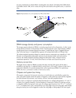
...2 DRAM storage density and power consumption 4 Memory access time...4 Chipsets and system bus timing...4 Memory bus speed...5 Burst mode ...17 Rambus DRAM ...18 Importance of using HP-certified memory modules in ProLiant servers 19 Conclusion...19 For more information...20 Call to action ...20 - Compaq ProLiant CL380 | Memory technology evolution: an overview of system memor - Page 2
performance gap prevents many applications from effectively using the full computing power of modern processors. In an attempt to narrow the performance gap, the industry vigorously pursues the development of new memory technologies. HP works with Joint Electronic Device Engineering Council (JEDEC - Compaq ProLiant CL380 | Memory technology evolution: an overview of system memor - Page 3
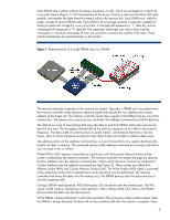
data in memory. The command portion of the address/command bus conveys instructions such as read, write, or refresh. When FPM or EDO memory writes data devices drive the data onto the memory bus. While DRAM is being refreshed, it cannot be accessed. If the processor makes a data request while the - Compaq ProLiant CL380 | Memory technology evolution: an overview of system memor - Page 4
and system bus timing All computer components that execute instructions or transfer data are controlled by a system bus clock. The system chipset controls the speed, or frequency, of the system bus clock and thus regulates the traffic between the processor, main memory, PCI bus, and other peripheral - Compaq ProLiant CL380 | Memory technology evolution: an overview of system memor - Page 5
MHz, a divider circuit can generate a PCI bus frequency of 33 MHz (system clock ÷ 3) and a multiplier circuit can generate a processor frequency of 400 MHz (system clock x 4). Computer cycles for data or instructions due to clock four consecutive 64-bit sections of memory are accessed, one after the - Compaq ProLiant CL380 | Memory technology evolution: an overview of system memor - Page 6
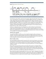
additional data sections are accessed with every clock cycle after the first access (6-1-1-1) before the memory controller has to send another CAS. Figure 4. Burst mode access. NOP is a "No Operation" instruction. Clock Command Address Data Active NOP NOP Read NOP NOP NOP NOP NOP NOP Row Col - Compaq ProLiant CL380 | Memory technology evolution: an overview of system memor - Page 7
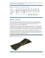
while one memory bank is being accessed, the other bank remains ready to be accessed. This allows the processor to initiate a new memory access MHz, SDRAM increases memory bandwidth to 800 MB/s, 50 percent more than EDO DRAMs (533 MB/s at 66 MHz). Registered SDRAM modules To achieve higher memory - Compaq ProLiant CL380 | Memory technology evolution: an overview of system memor - Page 8
and double-sided configurations, DIMMs are classified as single-rank or dual-rank. A memory rank is defined as an area or block of 64-bits created by using some are staggered so that both sets of DRAM chips do not contend for the memory bus at the same time. Quad-rank DIMMs with ECC produces four 72- - Compaq ProLiant CL380 | Memory technology evolution: an overview of system memor - Page 9
operation. To prevent this and other memory-related problems, customers should only use HP-certified DIMMs available in the memory option kits for each ProLiant server (see the "Importance of using HP-certified memory modules in ProLiant servers" section). Another important difference between single - Compaq ProLiant CL380 | Memory technology evolution: an overview of system memor - Page 10
prevent bank or rank interleaving. The effective throughput of the memory controller is the sum of the individual memory channels. As the number of cores on a single processor increases, the number of integrated memory controllers will need to increase accordingly to provide the necessary throughput - Compaq ProLiant CL380 | Memory technology evolution: an overview of system memor - Page 11
SDRAM, the growing performance gap between the memory and processor must be filled by more advanced memory technologies. These technologies, which are described based data bus, and SSTL_2 low voltage signaling. At 400 MHz, DDR increases memory bandwidth to 3.2 GB/s, which is 400 percent more than - Compaq ProLiant CL380 | Memory technology evolution: an overview of system memor - Page 12
specification known as Stub Series-Terminated Logic_2 (SSTL_2). This low-voltage signaling results in lower power valid on the SDRAM pins. The memory controller uses the data strobe signal setup times to a synchronous clock. Thus, at a data rate of 400 Mb/s, the command bus must operate at 200 MHz. 12 - Compaq ProLiant CL380 | Memory technology evolution: an overview of system memor - Page 13
used in desktop PCs or servers. To vary the cost of DDR-1 DIMMs for these different markets, memory manufacturers provide unbuffered and registered up to 6.4 GB/s, lower power consumption, and improvements in packaging. At 400 MHz and 800 Mb/s, DDR-2 increases memory bandwidth to 6.4 GB/s, which - Compaq ProLiant CL380 | Memory technology evolution: an overview of system memor - Page 14
support "write leveling" on DDR-3 DIMMs. • 1.5-V signaling (compared to 1.8 V for DDR-2) for lower power consumption • A thermal sensor integrated on the DIMM module signals the chipset to throttle memory MHz 133 MHz 166 MHz 200 MHz 200 MHz 266 MHz 333 MHz 400 MHz 400 MHz 533 MHz 667 MHz 800 MHz - Compaq ProLiant CL380 | Memory technology evolution: an overview of system memor - Page 15
the electrical signals from the memory controller to reach the the motherboard between the memory controller and memory slots. supported as the bus speed increases. For example, Figure 14 shows the number of loads supported of supported loads had two options: limit memory capacity so that fewer errors - Compaq ProLiant CL380 | Memory technology evolution: an overview of system memor - Page 16
Consequently, JEDEC developed the Fully-Buffered DIMM (FB-DIMM) specification, a serial interface that eliminates the parallel stub-bus topology and allows higher memory bandwidth while maintaining or increasing memory capacity. FB-DIMM architecture The FB-DIMM architecture has serial links between - Compaq ProLiant CL380 | Memory technology evolution: an overview of system memor - Page 17
power use (thermal load). Memory latency is the delay from the time the data is requested to the time when the data is available from the memory , a heat spreader is required to help draw heat away from the FB-DIMM so it can be cooled more efficiently by the server's internal fans (Figure 16). These - Compaq ProLiant CL380 | Memory technology evolution: an overview of system memor - Page 18
: RDRAMs, Rambus application-specific integrated circuits, and an 150 MHz to keep up with the packet transfer rate at 1.2 GHz. This allows for plenty of timing margin in the design of the memory controller. Figure 17. Rambus DRAM RDRAM is capable of supporting up to 32 RDRAM devices on one memory - Compaq ProLiant CL380 | Memory technology evolution: an overview of system memor - Page 19
-rank DIMMs. HP memory option kits are listed in each server's user guide and in the product QuickSpecs available at www.hp.com. Conclusion The increasing performance gap between processors and memory has generated development of several memory technologies. While some memory manufacturers prefer - Compaq ProLiant CL380 | Memory technology evolution: an overview of system memor - Page 20
refer to the resources listed below. Resource description JEDEC Web site HP Advanced Memory Protection Fully-Buffered DIMM technology in HP ProLiant servers Web address http://www.jedec.org http://h18004.www1.hp.com/products/servers/technology/whitepapers/advtechnology.html#mem http://h18004.www1
-
 1
1 -
 2
2 -
 3
3 -
 4
4 -
 5
5 -
 6
6 -
 7
7 -
8
-
9
-
10
-
11
-
12
-
13
-
14
-
15
-
16
-
17
-
18
-
19
-
20
 |
 |
Memory technology evolution: an overview
of system memory technologies
technology brief, 8
th
edition
Abstract
..............................................................................................................................................
2
Introduction
.........................................................................................................................................
2
Basic DRAM operation
.........................................................................................................................
2
DRAM storage density and power consumption
...................................................................................
4
Memory access time
.........................................................................................................................
4
Chipsets and system bus timing
..........................................................................................................
4
Memory bus speed
...........................................................................................................................
5
Burst mode access
............................................................................................................................
5
SDRAM technology
..............................................................................................................................
6
Bank interleaving
.............................................................................................................................
7
Increased bandwidth
........................................................................................................................
7
Registered SDRAM modules
..............................................................................................................
7
DIMM Configurations
.......................................................................................................................
8
Single-sided and double-sided DIMMs
............................................................................................
8
Single-rank, dual-rank, and quad-rank DIMMs
.................................................................................
8
Rank interleaving
..........................................................................................................................
9
Memory channel interleaving
..........................................................................................................
10
Advanced memory technologies
..........................................................................................................
11
Double Data Rate SDRAM technologies
............................................................................................
11
DDR-1
.......................................................................................................................................
11
DDR-2
.......................................................................................................................................
13
DDR-3
.......................................................................................................................................
14
Module naming convention and peak bandwidth
...........................................................................
14
Fully-Buffered DIMMs
......................................................................................................................
15
FB-DIMM architecture
..................................................................................................................
16
Challenges
................................................................................................................................
17
Rambus DRAM
..............................................................................................................................
18
Importance of using HP-certified memory modules in ProLiant servers
.......................................................
19
Conclusion
........................................................................................................................................
19
For more information
..........................................................................................................................
20
Call to action
....................................................................................................................................
20