HP ProLiant SL4540 Memory technology evolution: an overview of system memory t
HP ProLiant SL4540 Manual
 |
View all HP ProLiant SL4540 manuals
Add to My Manuals
Save this manual to your list of manuals |
HP ProLiant SL4540 manual content summary:
- HP ProLiant SL4540 | Memory technology evolution: an overview of system memory t - Page 1
...2 DRAM storage density and power consumption 4 Memory access time...4 Chipsets and system bus timing...4 Memory bus speed...5 Burst mode access...5 SDRAM technology ...6 Bank interleaving ...7 Increased bandwidth ...7 Registered SDRAM modules ...7 DIMM Configurations ...8 Single-sided and double - HP ProLiant SL4540 | Memory technology evolution: an overview of system memory t - Page 2
applications are driving the need for better memory technologies for servers and workstations. Consequently, there are several memory technologies on the market at any given time. HP evaluates developing memory technologies in terms of price, performance, and backward compatibility and implements - HP ProLiant SL4540 | Memory technology evolution: an overview of system memory t - Page 3
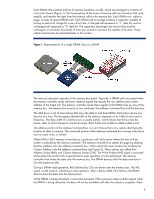
/command bus is a set of traces that carry signals identifying the location of data in memory. The command portion of the address/command bus conveys instructions such as read, write, or refresh. When FPM or EDO memory writes data to a particular cell, the location where the data will be written is - HP ProLiant SL4540 | Memory technology evolution: an overview of system memory t - Page 4
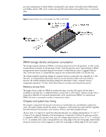
Representation of a write operation for FPM or EDO RAM DRAM storage density and power consumption The storage capacity (density) of DRAM is is converted to number of memory bus clocks. Chipsets and system bus timing All computer components that execute instructions or transfer data are controlled - HP ProLiant SL4540 | Memory technology evolution: an overview of system memory t - Page 5
For this reason, the components in a typical server are controlled by different clocks that run at additional clock cycles for data or instructions due to clock resynchronization. In contrast factors that control the speed of the memory subsystem are the memory timing and the maximum DRAM speed. Burst - HP ProLiant SL4540 | Memory technology evolution: an overview of system memory t - Page 6
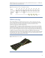
additional data sections are accessed with every clock cycle after the first access (6-1-1-1) before the memory controller has to send another CAS. Figure 4. Burst mode access. NOP is a "No Operation" instruction. Clock Command Address Data Active NOP NOP Read NOP NOP NOP NOP NOP NOP Row Col - HP ProLiant SL4540 | Memory technology evolution: an overview of system memory t - Page 7
Bank interleaving SDRAM divides memory into two to four banks for simultaneous access to more data. This division and simultaneous access is known as interleaving. Using a notebook analogy, two-way interleaving is like dividing each page in a notebook into two parts and having two assistants to each - HP ProLiant SL4540 | Memory technology evolution: an overview of system memory t - Page 8
DIMMs In addition to single-sided and double-sided configurations, DIMMs are classified as single-rank or dual-rank. A memory rank is defined as an area or block of staggered so that both sets of DRAM chips do not contend for the memory bus at the same time. Quad-rank DIMMs with ECC produces four 72 - HP ProLiant SL4540 | Memory technology evolution: an overview of system memory t - Page 9
. When an invalid memory configuration is detected, the system stops the boot process, thus avoiding unreliable operation. To prevent this and other memory-related problems, customers should only use HP-certified DIMMs available in the memory option kits for each ProLiant server (see the "Importance - HP ProLiant SL4540 | Memory technology evolution: an overview of system memory t - Page 10
controller successively provides a 64-byte cache line of data from the first DIMM on its channel. After the last memory controller completes the data transfer, the memory controllers can provide a cache line from a second DIMM on each channel. Channel interleaving does not prevent bank or rank - HP ProLiant SL4540 | Memory technology evolution: an overview of system memory t - Page 11
doubles the transfer rate without increasing the frequency of the memory clock. This section describes three generations of DDR SDRAM rate, DDR SDRAM uses a technique called prefetching to transfer two bits from the memory cell array to the I/O buffer in two separate pipelines. Then the I/O - HP ProLiant SL4540 | Memory technology evolution: an overview of system memory t - Page 12
specification known as Stub Series-Terminated Logic_2 (SSTL_2). This low-voltage signaling results in lower power consumption data strobe signal as data becomes valid on the SDRAM pins. The memory controller uses the data strobe signal to locate data more accurately and operate at 200 MHz. 12 - HP ProLiant SL4540 | Memory technology evolution: an overview of system memory t - Page 13
used in desktop PCs or servers. To vary the cost of DDR-1 DIMMs for these different markets, memory manufacturers provide unbuffered and registered versions up to 6.4 GB/s, lower power consumption, and improvements in packaging. At 400 MHz and 800 Mb/s, DDR-2 increases memory bandwidth to 6.4 GB/s, - HP ProLiant SL4540 | Memory technology evolution: an overview of system memory t - Page 14
support "write leveling" on DDR-3 DIMMs. • 1.5-V signaling (compared to 1.8 V for DDR-2) for lower power consumption • A thermal sensor integrated on the DIMM module signals the chipset to throttle memory PC3-12800 Bus speed 100 MHz 133 MHz 166 MHz 200 MHz 200 MHz 266 MHz 333 MHz 400 MHz 400 MHz 533 - HP ProLiant SL4540 | Memory technology evolution: an overview of system memory t - Page 15
traces on the motherboard between the memory controller and memory slots. Both the supported as the bus speed increases. For example, Figure 14 shows the number of loads supported number of supported loads drops from System designers had two options: limit memory capacity so that fewer errors occur - HP ProLiant SL4540 | Memory technology evolution: an overview of system memory t - Page 16
specification, a serial interface that eliminates the parallel stub-bus topology and allows higher memory bandwidth while maintaining or increasing memory between the memory controller and the FB-DIMMs, which are connected in a daisy chain configuration (Figure 15). Relative to the memory controller, - HP ProLiant SL4540 | Memory technology evolution: an overview of system memory t - Page 17
Additionally, the transmission latency, which exists for all memory technologies, increases due to the point-to-point server's internal fans (Figure 16). These concerns are driving the design of AMBs that use 15 to 20 percent less power, even though some manufacturers claim up to 40 percent power - HP ProLiant SL4540 | Memory technology evolution: an overview of system memory t - Page 18
consists of three key elements: RDRAMs, Rambus application-specific integrated circuits, and an interconnect called the Rambus in the design of the memory controller. Figure 17. Rambus DRAM RDRAM is capable of supporting up to 32 RDRAM devices on one memory channel while maintaining a 1.2-GHz - HP ProLiant SL4540 | Memory technology evolution: an overview of system memory t - Page 19
-rank DIMMs. HP memory option kits are listed in each server's user guide and in the product QuickSpecs available at www.hp.com. Conclusion The increasing performance gap between processors and memory has generated development of several memory technologies. While some memory manufacturers prefer - HP ProLiant SL4540 | Memory technology evolution: an overview of system memory t - Page 20
refer to the resources listed below. Resource description JEDEC Web site HP Advanced Memory Protection Fully-Buffered DIMM technology in HP ProLiant servers Web address http://www.jedec.org http://h18004.www1.hp.com/products/servers/technology/whitepapers/advtechnology.html#mem http://h18004.www1
-
 1
1 -
 2
2 -
 3
3 -
 4
4 -
 5
5 -
 6
6 -
 7
7 -
8
-
9
-
10
-
11
-
12
-
13
-
14
-
15
-
16
-
17
-
18
-
19
-
20
 |
 |

Memory technology evolution: an overview
of system memory technologies
technology brief, 8
th
edition
Abstract
..............................................................................................................................................
2
Introduction
.........................................................................................................................................
2
Basic DRAM operation
.........................................................................................................................
2
DRAM storage density and power consumption
...................................................................................
4
Memory access time
.........................................................................................................................
4
Chipsets and system bus timing
..........................................................................................................
4
Memory bus speed
...........................................................................................................................
5
Burst mode access
............................................................................................................................
5
SDRAM technology
..............................................................................................................................
6
Bank interleaving
.............................................................................................................................
7
Increased bandwidth
........................................................................................................................
7
Registered SDRAM modules
..............................................................................................................
7
DIMM Configurations
.......................................................................................................................
8
Single-sided and double-sided DIMMs
............................................................................................
8
Single-rank, dual-rank, and quad-rank DIMMs
.................................................................................
8
Rank interleaving
..........................................................................................................................
9
Memory channel interleaving
..........................................................................................................
10
Advanced memory technologies
..........................................................................................................
11
Double Data Rate SDRAM technologies
............................................................................................
11
DDR-1
.......................................................................................................................................
11
DDR-2
.......................................................................................................................................
13
DDR-3
.......................................................................................................................................
14
Module naming convention and peak bandwidth
...........................................................................
14
Fully-Buffered DIMMs
......................................................................................................................
15
FB-DIMM architecture
..................................................................................................................
16
Challenges
................................................................................................................................
17
Rambus DRAM
..............................................................................................................................
18
Importance of using HP-certified memory modules in ProLiant servers
.......................................................
19
Conclusion
........................................................................................................................................
19
For more information
..........................................................................................................................
20
Call to action
....................................................................................................................................
20