HP ProLiant SL6000 Memory technology evolution: an overview of system memory t
HP ProLiant SL6000 Manual
 |
View all HP ProLiant SL6000 manuals
Add to My Manuals
Save this manual to your list of manuals |
HP ProLiant SL6000 manual content summary:
- HP ProLiant SL6000 | Memory technology evolution: an overview of system memory t - Page 1
Double Data Rate SDRAM technologies 11 DDR-1 ...11 DDR-2 ...13 DDR-3 ...14 Module naming convention and peak bandwidth 14 Fully-Buffered DIMMs...15 FB-DIMM architecture...16 Challenges ...17 Rambus DRAM ...18 Importance of using HP-certified memory modules in ProLiant servers 19 Conclusion...19 - HP ProLiant SL6000 | Memory technology evolution: an overview of system memory t - Page 2
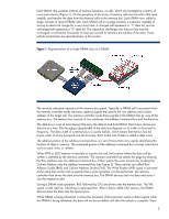
technologies on the market at any given time. HP evaluates developing memory technologies in terms of price, performance, and backward compatibility and implements the most promising technologies in ProLiant servers. HP drive to the system memory. Computers use two types of system memory-cache memory - HP ProLiant SL6000 | Memory technology evolution: an overview of system memory t - Page 3
/command bus is a set of traces that carry signals identifying the location of data in memory. The command portion of the address/command bus conveys instructions such as read, write, or refresh. When FPM or EDO memory writes data to a particular cell, the location where the data will be written is - HP ProLiant SL6000 | Memory technology evolution: an overview of system memory t - Page 4
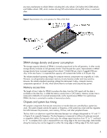
is converted to number of memory bus clocks. Chipsets and system bus timing All computer components that execute instructions or transfer data are controlled by a system bus clock. The system chipset controls the speed, or frequency, of the system bus clock and thus regulates the traffic between the - HP ProLiant SL6000 | Memory technology evolution: an overview of system memory t - Page 5
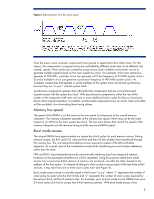
system bus clock. With asynchronous components, either the rest of the system or the component itself must wait one or more additional clock cycles for data or instructions . Burst mode access The original DRAM took approximately six system bus clock cycles for each memory access. During memory - HP ProLiant SL6000 | Memory technology evolution: an overview of system memory t - Page 6
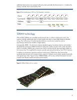
" instruction. Clock Command Address Data Active NOP NOP Read NOP NOP NOP NOP NOP NOP Row Col Data Data Data Data 64b 64b 64b 64b SDRAM technology FPM modules- developed the synchronous DRAM standard to reduce the number of system clock cycles required to read or write data. SDRAM uses - HP ProLiant SL6000 | Memory technology evolution: an overview of system memory t - Page 7
DRAM chip. Simultaneously, a phase lock loop chip on the registered DIMM generates a second clock signal that runs synchronously with the system bus clock. This prevents the system bus clock signal from having to drive all the DRAM chips, and it allows the addition of more memory modules to the - HP ProLiant SL6000 | Memory technology evolution: an overview of system memory t - Page 8
DIMM Configurations Single-sided and double-sided DIMMs Each DRAM chip on a DIMM provides either 4 bits or 8 bits of a 64-bit data word. Chips that provide 4 bits are called x4 (by 4), and chips that provide 8 bits are called x8 (by 8). It takes eight x8 chips or sixteen x4 chips to make a 64-bit - HP ProLiant SL6000 | Memory technology evolution: an overview of system memory t - Page 9
for faster memory technologies such as DDR2-667 capable of supporting two dual-rank system stops the boot process, thus avoiding unreliable operation. To prevent this and other memory-related problems, customers should only use HP-certified DIMMs available in the memory option kits for each ProLiant - HP ProLiant SL6000 | Memory technology evolution: an overview of system memory t - Page 10
Memory channel interleaving Multi-core processors running multi-threaded applications pose a significant challenge to the memory subsystem. The processor cores share the bandwidth of the memory bus; therefore, the multi-core processor's performance is limited by the memory bus bandwidth. Even with - HP ProLiant SL6000 | Memory technology evolution: an overview of system memory t - Page 11
high-speed processors (Figure 9). Figure 9. Peak bandwidth comparison of SDRAM and advanced SDRAM technologies Double Data Rate SDRAM technologies Double Data Rate (DDR) SDRAM is advantageous for systems that require higher bandwidth than can be obtained using SDRAM. Basically, DDR SDRAM doubles - HP ProLiant SL6000 | Memory technology evolution: an overview of system memory t - Page 12
SDRAM SSTL_2 low-voltage signaling technology Another difference between SDRAM and DDR-1 is the signaling technology. Instead of using a bus is capable of running at these speeds, the command bus cannot. Tight system timing requirements were alleviated on the data bus by using strobes. However, the - HP ProLiant SL6000 | Memory technology evolution: an overview of system memory t - Page 13
the load of all the DDR modules on the system memory bus, but they can be used in systems that do not require high memory capacity. Registered compatibility Because of their different data strobes, voltage levels, and signaling technologies, it is not possible to mix SDRAM and DDR-1 DIMMS within - HP ProLiant SL6000 | Memory technology evolution: an overview of system memory t - Page 14
stubs and their length. This feature requires the controller to support "write leveling" on DDR-3 DIMMs. • 1.5-V signaling (compared 133 MHz = 2.1 GB/s or 2100 MB/s). Table 1. Summary of DDR SDRAM technologies Type DDR-1 DDR-2 DDR-3 Component naming convention DDR200 DDR266 DDR333 DDR400 DDR2-400 - HP ProLiant SL6000 | Memory technology evolution: an overview of system memory t - Page 15
per channel that can be supported as the bus speed increases. For example, Figure 14 shows the number of loads supported per channel at data rates was not a viable option due to increased cost and board complexity. System designers had two options: limit memory capacity so that fewer errors occur - HP ProLiant SL6000 | Memory technology evolution: an overview of system memory t - Page 16
Consequently, JEDEC developed the Fully-Buffered DIMM (FB-DIMM) specification, a serial interface that eliminates the parallel stub-bus topology and allows higher memory bandwidth while maintaining or increasing memory capacity. FB-DIMM architecture The FB-DIMM architecture has serial links between - HP ProLiant SL6000 | Memory technology evolution: an overview of system memory t - Page 17
Additionally, the transmission latency, which exists for all memory technologies, increases due to the point-to-point interconnection of therefore, the cumulative transmission latency can be significant in a fully-scaled system. An FB-DIMM consumes almost 5 Watts more than a typical registered DDR2 - HP ProLiant SL6000 | Memory technology evolution: an overview of system memory t - Page 18
(Figure 17) has the lowest signal count of all of the memory technologies. RDRAM incorporates a packet protocol and is capable of operating at 800 MHz of the memory controller. Figure 17. Rambus DRAM RDRAM is capable of supporting up to 32 RDRAM devices on one memory channel while maintaining a 1.2- - HP ProLiant SL6000 | Memory technology evolution: an overview of system memory t - Page 19
option kits are listed in each server's user guide and in the product QuickSpecs available at www.hp.com. Conclusion The increasing performance gap between processors and memory has generated development of several memory technologies. While some memory manufacturers prefer a revolutionary approach - HP ProLiant SL6000 | Memory technology evolution: an overview of system memory t - Page 20
refer to the resources listed below. Resource description JEDEC Web site HP Advanced Memory Protection Fully-Buffered DIMM technology in HP ProLiant servers Web address http://www.jedec.org http://h18004.www1.hp.com/products/servers/technology/whitepapers/advtechnology.html#mem http://h18004.www1
-
 1
1 -
 2
2 -
 3
3 -
 4
4 -
 5
5 -
 6
6 -
 7
7 -
8
-
9
-
10
-
11
-
12
-
13
-
14
-
15
-
16
-
17
-
18
-
19
-
20
 |
 |
Memory technology evolution: an overview
of system memory technologies
technology brief, 8
th
edition
Abstract
..............................................................................................................................................
2
Introduction
.........................................................................................................................................
2
Basic DRAM operation
.........................................................................................................................
2
DRAM storage density and power consumption
...................................................................................
4
Memory access time
.........................................................................................................................
4
Chipsets and system bus timing
..........................................................................................................
4
Memory bus speed
...........................................................................................................................
5
Burst mode access
............................................................................................................................
5
SDRAM technology
..............................................................................................................................
6
Bank interleaving
.............................................................................................................................
7
Increased bandwidth
........................................................................................................................
7
Registered SDRAM modules
..............................................................................................................
7
DIMM Configurations
.......................................................................................................................
8
Single-sided and double-sided DIMMs
............................................................................................
8
Single-rank, dual-rank, and quad-rank DIMMs
.................................................................................
8
Rank interleaving
..........................................................................................................................
9
Memory channel interleaving
..........................................................................................................
10
Advanced memory technologies
..........................................................................................................
11
Double Data Rate SDRAM technologies
............................................................................................
11
DDR-1
.......................................................................................................................................
11
DDR-2
.......................................................................................................................................
13
DDR-3
.......................................................................................................................................
14
Module naming convention and peak bandwidth
...........................................................................
14
Fully-Buffered DIMMs
......................................................................................................................
15
FB-DIMM architecture
..................................................................................................................
16
Challenges
................................................................................................................................
17
Rambus DRAM
..............................................................................................................................
18
Importance of using HP-certified memory modules in ProLiant servers
.......................................................
19
Conclusion
........................................................................................................................................
19
For more information
..........................................................................................................................
20
Call to action
....................................................................................................................................
20