ASRock 775Twins-HDTV Quick Installation Guide - Page 13
English, 7 Onboard Headers and Connectors - bios update
 |
View all ASRock 775Twins-HDTV manuals
Add to My Manuals
Save this manual to your list of manuals |
Page 13 highlights
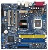
Jumper Setting Description PS2_USB_PWR1 Short pin2, pin3 to enable (see p.2 No. 1) +5VSB (standby) for PS/2 or USB wake up events. Note: To select +5VSB, it requires 2 Amp and higher standby current provided by power supply. JR1(see p.2 No. 28) JL1(see p.2 No. 28) Note: If the jumpers JL1 and JR1 are short, both the front panel and the rear panel audio connectors can work. Clear CMOS (CLRCMOS1, 3-pin jumper) (see p.2 No. 22) Default Clear CMOS Note: CLRCMOS1 allows you to clear the data in CMOS. The data in CMOS includes system setup information such as system password, date, time, and system setup parameters. To clear and reset the system parameters to default setup, please turn off the computer and unplug the power cord from the power supply. After waiting for 15 seconds, use a jumper cap to short pin2 and pin3 on CLRCMOS1 for 5 seconds. However, please do not clear the CMOS right after you update the BIOS. If you need to clear the CMOS when you just finish updating the BIOS, you must boot up the system first, and then shut it down before you do the clear-CMOS action. 2.7 Onboard Headers and Connectors Onboard headers and connectors are NOT jumpers. Do NOT place jumper caps over these headers and connectors. Placing jumper caps over the headers and connectors will cause permanent damage of the motherboard! FDD connector (33-pin FLOPPY1) (see p.2 No. 23) the red-striped side to Pin1 Note: Make sure the red-striped side of the cable is plugged into Pin1 side of the connector. Primary IDE Connector (Blue) Secondary IDE Connector (Black) (39-pin IDE1, see p.2, No. 8) (39-pin IDE2, see p.2, No. 9) English connect the blue end connect the black end to the motherboard to the IDE devices 80-conductor ATA 66/100/133 cable 13 ASRock 775Twins-HDTV Motherboard
-
 1
1 -
2
-
3
-
4
-
5
-
6
-
7
-
 8
8 -
 9
9 -
 10
10 -
 11
11 -
 12
12 -
 13
13 -
 14
14 -
 15
15 -
 16
16 -
 17
17 -
 18
18 -
19
-
20
-
21
-
22
-
23
-
24
-
25
-
26
-
27
-
28
-
29
-
30
-
31
-
32
-
33
-
34
-
35
-
36
-
37
-
38
-
39
-
40
-
41
-
42
-
43
-
44
-
45
-
46
-
47
-
48
-
49
-
50
-
51
-
52
-
53
-
54
-
55
-
56
-
57
-
58
-
59
-
60
-
61
-
62
-
63
-
64
-
65
-
66
-
67
-
68
-
69
-
70
-
71
-
72
-
73
-
74
-
75
-
76
-
77
-
78
-
79
-
80
-
81
-
82
-
83
-
84
-
85
-
86
-
87
-
88
-
89
-
90
-
91
-
92
-
93
-
94
-
95
-
96
-
97
-
98
-
99
-
100
-
101
-
102
-
103
-
104
-
105
-
106
-
107
-
108
-
109
-
110
-
111
-
112
-
113
-
114
-
115
-
116
-
117
-
118
-
119
-
120
-
121
-
122
-
123
-
124
-
125
-
126
-
127
-
128
-
129
 |
 |
