Asus P4SE P4SE User Manual - Page 48
Chip Configuration
 |
View all Asus P4SE manuals
Add to My Manuals
Save this manual to your list of manuals |
Page 48 highlights
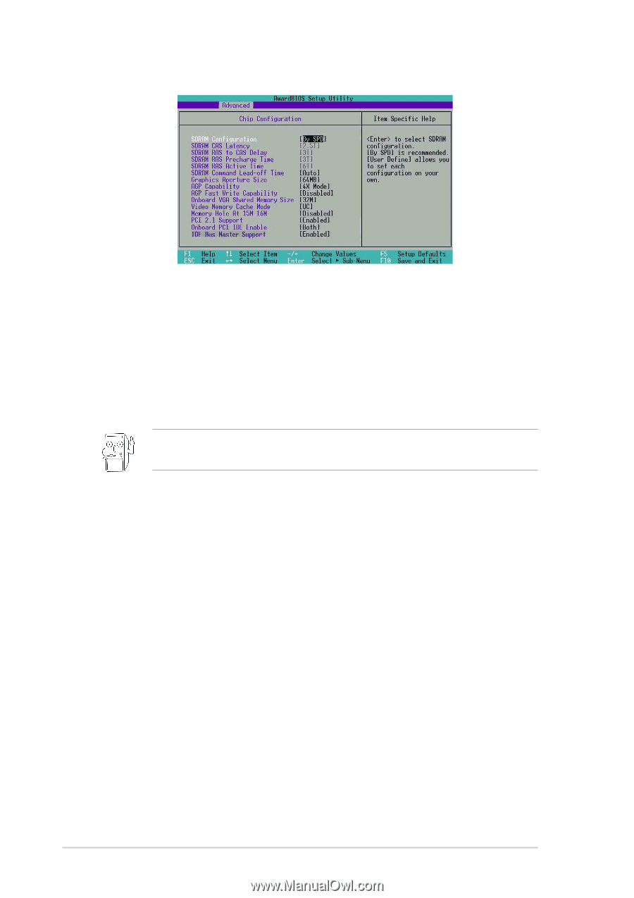
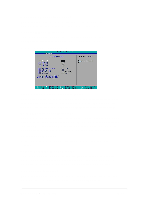
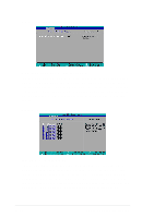
2.4.1 Chip Configuration SDRAM Configuration [By SPD] This parameter allows you to set the optimal timings for items 2-5, depending on the memory modules that you are using. The default setting is [By SPD], which configures items 2-5 by reading the contents in the SPD (Serial Presence Detect) device. The EEPROM on the memory module stores critical information about the module, such as memory type, size, speed, voltage interface, and module banks. Configuration options: [User Defined] [By SPD] The SDRAM parameters (items 2~5) become configurable only when you set the SDRAM Configuration to [User Defined]. SDRAM CAS Latency [2.5T] This item controls the latency between the SDRAM read command and the time the data actually becomes available. SDRAM RAS to CAS Delay [3T] This item controls the latency between the DDR SDRAM active command and the read/write command. SDRAM RAS Precharge Time [3T] This item controls the idle clocks after issuing a precharge command to the DDR SDRAM. SDRAM RAS Active Time [6T] This item controls the number of DDR SDRAM clocks used for DDR SDRAM parameters. SDRAM Command Lead-off Time [Auto] When set to [2T], memory read/write commands are issued 1 clock cycle behind the memory address (MA). When set to [1T], read/write commands and MA are issued simultaneously. Configuration options: [Auto] [2T] [1T] 2-14 Chapter 2: BIOS Information
-
 1
1 -
2
-
3
-
4
-
5
-
6
-
7
-
8
-
9
-
10
-
11
-
12
-
13
-
14
-
15
-
16
-
17
-
18
-
19
-
20
-
21
-
22
-
23
-
24
-
25
-
26
-
27
-
28
-
29
-
30
-
31
-
32
-
33
-
34
-
35
-
36
-
37
-
38
-
39
-
40
-
41
-
42
-
 43
43 -
 44
44 -
 45
45 -
 46
46 -
 47
47 -
 48
48 -
 49
49 -
 50
50 -
 51
51 -
 52
52 -
 53
53 -
54
-
55
-
56
-
57
-
58
-
59
-
60
-
61
-
62
-
63
-
64
-
65
-
66
-
67
-
68
-
69
-
70
 |
 |