Foxconn M61PML English Manual - Page 33
Advanced Chipset Features
 |
View all Foxconn M61PML manuals
Add to My Manuals
Save this manual to your list of manuals |
Page 33 highlights
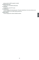
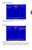
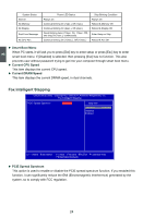
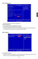
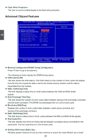
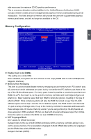
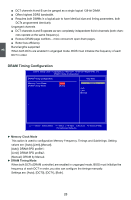
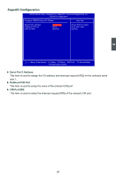
► Flash Write Protection This item is used to enable/disable to the flash write protection. Advanced Chipset Features CMOS Setup Utility - Copyright (C) 1985-2011, American Megatrends, Inc. Advanced Chipset Features Northbridge Chipset Configuration Help Item ► Memory Configuration [Press Enter] ► DRAM Timing Configuration [Press Enter] CAS Latency (Tcl) : N/A , 9 CLK RAS/CAS Delay (Trcd) : N/A , 9 CLK Row Precharge Time (Trp) :N/A , 9 CLK Min Active RAS (Tras) :N/A , 24 CLK RAS/RAS Delay (Trrd) :N/A , 4 CLK Row Cycle (Trc) :N/A , 33 CLK OnChip VGA Frame Buffer Size [128MB] 3 Move Enter:Select +/-/:Value F10:Save ESC:Exit F1:General Help F9:Optimized Defaults ► Memory Configuration/DRAM Timing Configuration Press to go to its submenu. The following six items display the DRAM timing values. ► CAS Latency(Tcl) This item shows the CAS latency. The CAS Latency is the number of clock cycles that elapse from the time the request for data is sent to the actual memory location until the data is transmitted from the module. ► RAS / CAS Delay(Trcd) This item displays a delay time (in clock cycles) between the CAS and RAS strobe signals. ► Row Precharge Time(Trp) This item shows the number of clock cycles taken between issuing of the precharge command and the active command. The DRAM row precharge time is in unit of clock cycle. ► Min Active RAS(Tras) Displays the number of clock cycles taken between a bank active command and issuing of the precharge command. ► RAS / RAS Delay(Trrd) This item shows a delay time (in clock cycles) between the RAS and RAS strobe signals. ► Row Cycle(Trc) This item displays the minimum timing interval between successive active commands to the same bank. The row cycle time is in unit of clock cycle. ► OnChip VGA Frame Buffer Size Allocates system memory for use as video memory to ensure the most efficient use of avail- 26
-
 1
1 -
2
-
3
-
4
-
5
-
6
-
7
-
8
-
9
-
10
-
11
-
12
-
13
-
14
-
15
-
16
-
17
-
18
-
19
-
20
-
21
-
22
-
23
-
24
-
25
-
26
-
27
-
 28
28 -
 29
29 -
 30
30 -
 31
31 -
 32
32 -
 33
33 -
 34
34 -
 35
35 -
 36
36 -
 37
37 -
 38
38 -
39
-
40
-
41
-
42
-
43
-
44
-
45
-
46
-
47
-
48
-
49
-
50
-
51
-
52
-
53
-
54
-
55
-
56
-
57
-
58
-
59
-
60
-
61
-
62
-
63
-
64
-
65
-
66
-
67
-
68
-
69
-
70
-
71
-
72
-
73
-
74
-
75
-
76
-
77
-
78
-
79
-
80
-
81
-
82
-
83
-
84
-
85
-
86
-
87
-
88
-
89
-
90
-
91
-
92
-
93
-
94
-
95
-
96
-
97
-
98
-
99
-
100
-
101
 |
 |