HP DL360 Memory technology evolution: an overview of system memory technologie - Page 4
DRAM storage density and power consumption, Memory access time, Chipsets and system bus timing
 |
UPC - 613326948835
View all HP DL360 manuals
Add to My Manuals
Save this manual to your list of manuals |
Page 4 highlights
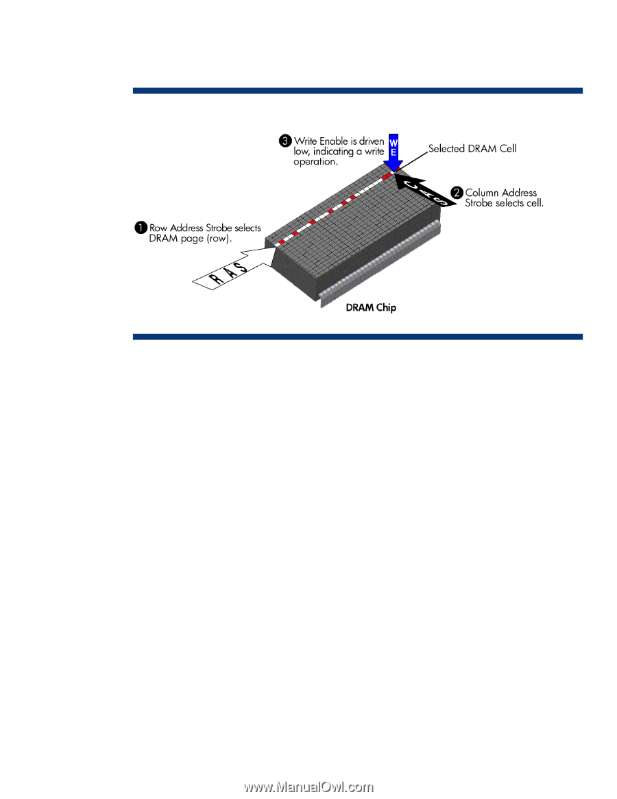
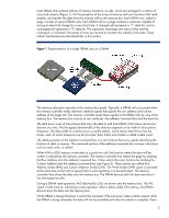
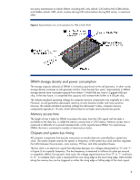
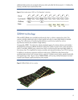
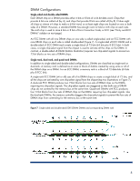
are many mechanisms to refresh DRAM, including RAS only refresh, CAS before RAS (CBR) refresh, and Hidden refresh. CBR, which involves driving CAS active before driving RAS active, is used most often. Figure 2. Representation of a write operation for FPM or EDO RAM DRAM storage density and power consumption The storage capacity (density) of DRAM is inversely proportional to the cell geometry. In other words, storage density increases as cell geometry shrinks. Over the past few years, improvements in DRAM storage density have increased capacity from almost 1 kilobit (Kb) per chip to 2 gigabit (Gb) per chip. In the near future, it is expected that capacity will increase even further to 4 Gb per chip. The industry-standard operating voltage for computer memory components was originally at 5 volts. However, as cell geometries decreased, memory circuitry became smaller and more sensitive. Likewise, the industry-standard operating voltage has decreased. Today, computer memory components operate at 1.8 volts, which allows them to run faster and consume less power. Memory access time The length of time it takes for DRAM to produce the data, from the CAS signal until the data is available on the data bus, is called the memory access time or CAS Latency. Memory access time is measured in billionths of a second (nanoseconds, ns) for asynchronous DRAM. For synchronous DRAM, the time is converted to number of memory bus clocks. Chipsets and system bus timing All computer components that execute instructions or transfer data are controlled by a system bus clock. The system chipset controls the speed, or frequency, of the system bus clock and thus regulates the traffic between the processor, main memory, PCI bus, and other peripheral buses. The bus clock is an electronic signal that alternates between two voltages (designated as "0" and "1" in Figure 3) at a specific frequency. The bus frequency is measured in millions of cycles per second, or megahertz (MHz). During each clock cycle, the voltage signal transitions from "0" to "1" and back to "0". A complete clock cycle is measured from one rising edge to the next rising edge. Data transfer along the memory bus can be triggered on either the rising edge or falling edge of the clock signal. 4
-
 1
1 -
 2
2 -
 3
3 -
 4
4 -
 5
5 -
 6
6 -
 7
7 -
 8
8 -
 9
9 -
 10
10 -
11
-
12
-
13
-
14
-
15
-
16
-
17
-
18
-
19
-
20
 |
 |