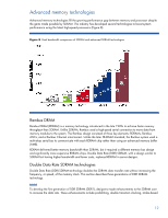
HP ProLiant SL390s Memory technology evolution: an overview of system memory t - Page 14
DDR3, Module naming convention and peak bandwidth,
 |
View all HP ProLiant SL390s manuals
Add to My Manuals
Save this manual to your list of manuals |
Page 14 highlights
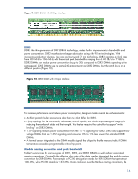
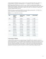
Figure 9. DDR2 DIMM with 240-pin interface DDR3 DDR3, the third-generation of DDR SDRAM technology, makes further improvements in bandwidth and power consumption. DDR3 manufacturers began fabrication using with 90 nm technologies. With increasing production volumes, they are moving toward 70 nm technology. DDR3 operates at clock rates from 400 MHz to 1066 MHz with theoretical peak bandwidths ranging from 6.40 GB/s to 17 GB/s. DDR3 DIMMs can reduce power consumption by up to 30% compared to DDR2 DIMMs operating at the same speed. DDR3 DIMMs use the same 240-pin connector as DDR2 DIMMs, but the notch key is in a different position (Figure 10). Figure 10. DDR3 DIMM with 240-pin interface To increase performance and reduce power consumption, designers made several key enhancements: • An 8-bit prefetch buffer stores more data than the 4-bit buffer for DDR2. • Fly-by topology for the commands, addresses, control signals, and clocks improves signal integrity by reducing the number of stubs and their length. This feature requires the controller to support "write leveling" on DDR3 DIMMs. • 1.5-V signaling reduces power consumption from the 1.8- V signaling for DDR2. DDR3 also supports low voltage DIMMs that use 1.35-V signaling and consume 10% to 15% less power than standard DDR3 DIMMs. • A thermal sensor integrated on the DIMM module signals the chipset to throttle memory traffic if DIMM temperature exceeds a programmable critical trip point. Module naming convention and peak bandwidth Table 2 summarizes the various types of DDR1, DDR2, and DDR3 SDRAM as well as their associated naming conventions. Originally, the effective clock rate of the data transfer determined the module naming convention for DDR-SDRAM. For example, a PC200 designation stands for DDR SDRAM that operates at 100 MHz, while PC266 stands for 133 MHz. Dueto confusion over the Rambus naming convention, the 14
-
 1
1 -
2
-
3
-
4
-
5
-
6
-
7
-
8
-
 9
9 -
 10
10 -
 11
11 -
 12
12 -
 13
13 -
 14
14 -
 15
15 -
 16
16 -
 17
17 -
 18
18 -
 19
19
 |
 |
