Intel D845PEBT2 Specification Update - Page 14
Engineering Change Notice ECN Addition of the SMBus to the PCI Connector - connectors pin out
 |
View all Intel D845PEBT2 manuals
Add to My Manuals
Save this manual to your list of manuals |
Page 14 highlights
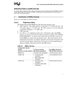
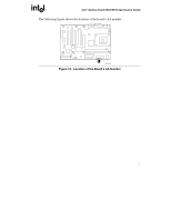
Intel Desktop Board D845PEBT2 Specification Update ✏ NOTE The SMBus routing to the PCI bus connectors does not conform to the PCI Engineering Change Notice (ECN) "Addition of the SMBus to the PCI Connector ECN", dated October 5th, 2000. The ECN specifies that SMBus signals must be routed to all PCI bus connectors. On this board, SMBus signals are routed to PCI bus connector 1 or 2 only (See Table 29). Add-in cards that implement PCI bus connector pins A40 and A41 for any purpose other than SMBCLK (SMBus clock) and SMBDAT (SMBus data) should not be installed in either PCI bus connector 1 or 2 depending on the board configuration (See Table 29). For information about Addition of the SMBus to the PCI Connector ECN Refer to http://www.pcisig.com/data/s pecifications/smb_ecn_0405 01.pdf ✏ NOTE This document references back-panel slot numbering with respect to processor location on the Desktop Board D845PEBT2. The AGP slot is not numbered. PCI slots are identified as PCI slot #x, starting with the slot closest to the processor. The ATX specification identifies expansion slot locations with respect to the far edge of a full-sized ATX chassis. The ATX specification and the Desktop Board D845PEBT2's silkscreen are opposite and could cause confusion. The ATX numbering convention is made without respect to slot type (PCI vs. AGP), but refers to an actual slot location on a chassis. Figure 14 on page 61 illustrates the Desktop Board D845PEBT2's PCI slot numbering. 8
-
 1
1 -
2
-
3
-
4
-
5
-
6
-
7
-
8
-
 9
9 -
 10
10 -
 11
11 -
 12
12 -
 13
13 -
 14
14 -
 15
15 -
 16
16
 |
 |