Intel E6300 Data Sheet
Intel E6300 - Core 2 Duo Dual-Core Processor Manual
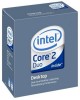 |
UPC - 735858184649
View all Intel E6300 manuals
Add to My Manuals
Save this manual to your list of manuals |
Intel E6300 manual content summary:
- Intel E6300 | Data Sheet - Page 1
Intel® Pentium® Dual-Core Processor E6000 and E5000 Series Datasheet November 2010 Document Number: 320467-011 - Intel E6300 | Data Sheet - Page 2
of any features or instructions marked "reserved" or "undefined." Intel reserves these for future definition and shall have no responsibility whatsoever for conflicts or incompatibilities arising from future changes to them. The Intel Pentium® dual-core processor E5000 and E6000 series - Intel E6300 | Data Sheet - Page 3
24 2.7.3.1 Platform Environment Control Interface (PECI) DC Specifications..... 25 2.7.3.2 GTL+ Front Side Bus Specifications 26 2.8 Clock Specifications 27 2.8.1 Front Side Bus Clock (BCLK[1:0]) and Processor Clocking 27 2.8.2 FSB Frequency Select Signals (BSEL[2:0 28 2.8.3 Phase Lock - Intel E6300 | Data Sheet - Page 4
Specifications 83 5.3.2.1 PECI Device Address 83 5.3.2.2 PECI Command Support 83 5.3.2.3 PECI Fault Handling Requirements 83 5.3.2.4 PECI GetTemp0() Error Code Support 83 6 Features ...85 6.1 Power-On Configuration Options 85 6.2 Clock Control and Low Power States 85 6.2.1 Normal State 86 - Intel E6300 | Data Sheet - Page 5
38 10 Intel® Pentium® Dual-Core Processor E6000 Series Top-Side Markings Example 39 11 Processor Land Coordinates and Quadrants, Top View 40 12 land-out Diagram (Top View - Left Side 42 13 land-out Diagram (Top View - Right Side 43 14 Processor Series Thermal Profile 77 15 Case Temperature (TC - Intel E6300 | Data Sheet - Page 6
27 15 Core Frequency to FSB Multiplier Configuration 28 16 BSEL[2:0] Frequency Table for BCLK[1:0 29 17 Front Side Bus Differential BCLK Specifications 29 18 FSB Differential Clock Specifications (800 MHz FSB 30 19 FSB Differential Clock Specifications (1066 MHz FSB 30 20 Processor Loading - Intel E6300 | Data Sheet - Page 7
80 GHz (Intel® Pentium® Dual-Core processor E6000 series) • Enhanced Intel Speedstep® Technology • Supports Intel® 64 architecture • Supports Intel® Virtualization Technology (Intel® VT) (Intel® Pentium® Dual-Core processor E6000 series only) • Supports Execute Disable Bit capability • FSB frequency - Intel E6300 | Data Sheet - Page 8
• Added Intel® Pentium® dual-core processor E5400 • Added Intel® Pentium® dual-core processor E6300 • Added Intel® Pentium® dual-core processor E6500 • Added Intel® Pentium® dual-core processor E6600 • Added Intel® Pentium® dual-core processor E5500 • Added Intel® Pentium® dual-core processor E6700 - Intel E6300 | Data Sheet - Page 9
3 (SSSE3). The processors support several Advanced Technologies: Execute Disable Bit, Intel® 64 architecture, and Enhanced Intel SpeedStep® Technology. The Intel® Pentium® dual-core processor E6000 series supports Intel® Virtualization Technology (Intel® VT). The processor's front side bus (FSB) use - Intel E6300 | Data Sheet - Page 10
is the generic form of the Intel® Pentium® dual-core processor E5000 and E6000 series. • Voltage Regulator Design Guide - For this document "Voltage Regulator Design Guide" may be used in place of: - Voltage Regulator-Down (VRD) 11.0 Processor Power Delivery Design Guidelines For Desktop LGA775 - Intel E6300 | Data Sheet - Page 11
Core™2 Duo processor E8000 and E7000 Series, and Intel® Pentium® Dual-Core Processor E6000 and E5000 Series Thermal and Mechanical Design Guidelines Voltage Regulator-Down (VRD) 11.0 Processor Power Delivery Design Guidelines For Desktop LGA775 Socket LGA775 Socket Mechanical Design Guide Intel® 64 - Intel E6300 | Data Sheet - Page 12
Introduction 12 Datasheet - Intel E6300 | Data Sheet - Page 13
the Voltage Regulator-Down (VRD) 11.0 Processor Power Delivery Design Guidelines For Desktop LGA775 Socket for further information. Contact your Intel field representative for additional information. VTT Decoupling Decoupling must be provided on the motherboard. Decoupling solutions must be sized to - Intel E6300 | Data Sheet - Page 14
in Table 4. See the Intel® Pentium® dualcore Processor E6000 and E5000 Series Specification Update for further details on specific valid core frequency and VID values of the processor. Note that this differs from the VID employed by the processor during a power management event (Thermal Monitor - Intel E6300 | Data Sheet - Page 15
Electrical Specifications Table 2. Voltage Identification Definition VID VID VID VID VID VID VID VID 76543210 Voltage 00000000 OFF 00000010 1.6 0 0 0 0 0 1 0 0 1.5875 0 0 0 0 0 1 1 0 1.575 0 0 0 0 1 0 0 0 1.5625 00001010 1.55 0 0 0 0 1 1 0 0 1.5375 0 0 0 0 1 1 1 0 1.525 0 0 0 1 0 0 0 - Intel E6300 | Data Sheet - Page 16
. A resistor must be used when tying bidirectional signals to power or ground. When tying any signal to power or ground, a resistor will also allow for system testability. Resistor values should be within ± 20% of the impedance of the motherboard trace for front side bus signals. For unused GTL - Intel E6300 | Data Sheet - Page 17
or electric fields. Absolute Maximum and Minimum Ratings Symbol Parameter Min VCC Core voltage with respect to VSS -0.3 VTT FSB termination voltage with respect to VSS -0.3 TCASE Processor case temperature See Section 5 TSTORAGE Processor storage temperature -40 Max 1.45 1.45 - Intel E6300 | Data Sheet - Page 18
GHz E6600 3.06 GHz E6500 2.93 GHz E6300 2.80 GHz See Table 5, Figure 1 V E5200 2.50 GHz E5300 2.66 GHz E5400 2.70 GHz E5500 2.80 GHz E5700 3.00 GHz E5800 3.20 GHz VCC_BOOT VCCPLL ICC Default VCC voltage for initial power up - 1.10 - V PLL VCC - 5% 1.50 + 5% V Processor - Intel E6300 | Data Sheet - Page 19
range. Note that this differs from the VID employed by the processor during a power management event (Thermal Monitor 2, Enhanced Intel SpeedStep technology, or Extended HALT State). 2. Unless otherwise noted, all specifications in this table are based on estimates and simulations or empirical - Intel E6300 | Data Sheet - Page 20
Guide for socket loadline guidelines and VR implementation details. 4. Adherence to this loadline specification is required to ensure reliable processor operation. Processor 60 65 70 75 Vcc Maximum Vcc Typical Vcc Minimum NOTES: 1. The loadline specification includes both static and transient - Intel E6300 | Data Sheet - Page 21
defined as VTT. Because platforms implement separate power planes for each processor (and chipset), separate VCC and VTT supplies motherboard (see Table 14 for GTLREF specifications). Termination resistors (RTT) for GTL+ signals are provided on the processor silicon and are terminated to VTT. Intel - Intel E6300 | Data Sheet - Page 22
Specifications 2.7.1 FSB Signal Groups The front side bus signals have been combined into groups by buffer type / Output FSB Clock Power/Other Synchronous to BCLK[1:0] Clock ADSTB[1:0]#, processor systems where no debug port is implemented on the system board, these signals are used to support - Intel E6300 | Data Sheet - Page 23
Electrical Specifications . Table 8. Table 9. 2.7.2 Signal Characteristics Signals with RTT A[35:3]#, ADS#, ADSTB[1:0]#, least eight BCLKs in order for the processor to recognize the proper signal state. See Section 2.7.3 for the DC specifications. See Section 6.2 for additional timing - Intel E6300 | Data Sheet - Page 24
Table 11. Processor DC Specifications The processor DC specifications in this section are defined at the processor core (pads) unless otherwise stated. All specifications apply to all frequencies and cache sizes unless otherwise stated. GTL+ Signal Group DC Specifications Symbol Parameter Min - Intel E6300 | Data Sheet - Page 25
Specifications PECI is an Intel proprietary one-wire interface that provides a communication channel between Intel processors, chipsets, and external thermal monitoring devices. The processor of relative processor temperature. PECI provides an interface to relay the highest DTS temperature within a - Intel E6300 | Data Sheet - Page 26
does not affect VTT min/max specifications. See Table 4 for VTT specifications. 2. The leakage specification applies to powered devices on the PECI bus. + Front Side Bus Specifications In most cases, termination resistors are not required as these are integrated into the processor silicon. See Table - Intel E6300 | Data Sheet - Page 27
+ output driver. 4. COMP resistance must be provided on the system board with 1% resistors. COMP[3:0] and COMP8 resistors are to VSS. 2.8 Clock Specifications 2.8.1 Front Side Bus Clock (BCLK[1:0]) and Processor Clocking BCLK[1:0] directly controls the FSB interface speed as well as the core - Intel E6300 | Data Sheet - Page 28
with each combination. The required frequency is determined by the processor, chipset, and clock synthesizer. All agents must operate at the same frequency. The Intel® Pentium® dual-core processor E5000 series operates at a 800 MHz FSB frequency (selected by a 200 MHz BCLK[1:0] frequency). The - Intel E6300 | Data Sheet - Page 29
An on-die PLL filter solution will be implemented on the processor. The VCCPLL input is used for the PLL. See Table 4 for DC specifications. 2.8.4 BCLK[1:0] Specifications Table 17. Front Side Bus Differential BCLK Specifications Symbol Parameter Min Typ Max Unit Figure Notes1 VL Input - Intel E6300 | Data Sheet - Page 30
FSB Differential Clock Specifications (1066 MHz FSB otherwise noted, all specifications in this table apply to all processor core frequencies based on a specification is based on the summation of +300 PPM deviation from a 3.75 ns period and a +0.5% maximum variance due to spread spectrum clocking - Intel E6300 | Data Sheet - Page 31
Electrical Specifications Figure 3. Differential Clock Waveform Threshold Region Tph BCLK1 VCROSS (ABS) VCROSS (ABS) Edge Ringback Falling Edge Ringback VL Undershoot Figure 4. Measurement Points for Differential Clock Waveforms +150 mV 0.0 V -150 mV Diff Slew_rise V_swing Slew _fall - Intel E6300 | Data Sheet - Page 32
Electrical Specifications 32 Datasheet - Intel E6300 | Data Sheet - Page 33
Package Mechanical Specifications 3 Package Mechanical Specifications Figure 5. The processor is packaged in a Flip-Chip Land Grid Array (FC-LGA8) package that interfaces with the motherboard using an LGA775 socket. The package consists of a processor core mounted on a substrate land-carrier. An - Intel E6300 | Data Sheet - Page 34
Figure 6. Processor Package Drawing Sheet 1 of 3 Package Mechanical Specifications 34 Datasheet - Intel E6300 | Data Sheet - Page 35
Package Mechanical Specifications Figure 7. Processor Package Drawing Sheet 2 of 3 Datasheet 35 - Intel E6300 | Data Sheet - Page 36
Figure 8. Processor Package Drawing Sheet 3 of 3 Package Mechanical Specifications 36 Datasheet - Intel E6300 | Data Sheet - Page 37
or load-bearing surface for thermal and mechanical solution. The minimum loading specification must be maintained by any thermal and mechanical solutions. Processor Loading Specifications Parameter Minimum Maximum Notes Static 80 N [17 lbf] 311 N [70 lbf] 1, 2, 3 Dynamic - 756 N [170 lbf - Intel E6300 | Data Sheet - Page 38
9 and Figure 10 show the top-side markings on the processor. These diagrams can be used to aid in the identification of the processor. Intel® Pentium® Dual-Core Processor E5000 Series Top-Side Markings Example INTEL ©M'06 E5200 Intel® Pentium® Dual-Core SLAY7 [COO] 2.50GHZ/2M/800/06 [FPO] e4 ATPO - Intel E6300 | Data Sheet - Page 39
Package Mechanical Specifications Figure 10. Intel® Pentium® Dual-Core Processor E6000 Series Top-Side Markings Example INTEL ©M'06 E6300 Intel® Pentium® Dual-Core SLGU9 [COO] 2.80GHZ/2M/1066/06 [FPO] e4 ATPO S/N Datasheet 39 - Intel E6300 | Data Sheet - Page 40
AM AL AK AJ AH AG AF AE AD AC AB AA Y W V Socket 775 U T Quadrants R P Top View N M L K J H G F E D C B A 30 29 28 27 26 25 24 23 22 21 20 19 18 17 16 15 14 13 12 11 10 9 8 7 6 5 4 3 2 1 V / Clocks TT Data AN AM AL AK AJ AH AG AF AE AD AC - Intel E6300 | Data Sheet - Page 41
and Signal Descriptions 4 4.1 Land Listing and Signal Descriptions This chapter provides the processor land assignment and signal descriptions. Processor Land Assignments This section contains the land listings for the processor. The land-out footprint is shown in Figure 12 and Figure 13. These - Intel E6300 | Data Sheet - Page 42
Land Listing and Signal Descriptions Figure 12. land-out Diagram (Top View - Left Side) 30 29 28 27 26 25 24 23 22 21 20 19 18 17 16 15 AN VCC VCC VSS VSS VCC VCC VSS VSS VCC VCC VSS VCC VCC VSS VSS VCC AM VCC VCC VSS VSS VCC VCC VSS VSS VCC VCC VSS VCC VCC - Intel E6300 | Data Sheet - Page 43
Land Listing and Signal Descriptions Figure 13. land-out Diagram (Top View - Right Side) 14 VCC VCC VCC VCC VCC VCC VCC VCC VCC 13 VSS VSS VSS VSS VSS VSS VSS VSS VSS VCC VCC VSS VSS 12 VCC VCC VCC VCC VCC VCC VCC VCC VCC VCC VSS 11 VCC VCC VCC VCC VCC VCC VCC VCC VCC 10 VSS VSS VSS VSS VSS - Intel E6300 | Data Sheet - Page 44
Input/Output R6 Source Synch Input/Output AD5 Source Synch Input/Output F28 Clock Input G28 Clock Input Table 23. Alphabetical Land Assignments Land Name Land Signal Buffer # Type Direction BNR# BPM0# BPM1# BPM2# BPM3# BPM4# BPM5# BPRI# BR0# BSEL0 BSEL1 BSEL2 COMP0 COMP1 COMP2 COMP3 - Intel E6300 | Data Sheet - Page 45
Synch Input/Output Table 23. Alphabetical Land Assignments Land Name Land Signal Buffer # Type Direction D61# D62# D63# DBI0# DBI1# DBI2# DBI3# DBR# DBSY# Power/Other Output B2 Common Clock Input/Output G7 Common Clock Input T2 Asynch CMOS Input P1 Asynch CMOS Input C1 Common Clock - Intel E6300 | Data Sheet - Page 46
Buffer # Type Direction FC31 Power/Other H15 Power/Other H16 Power/Other J17 Power/Other H4 Power/Other AD3 Power/Other AB3 Power/Other G10 Power/Other AA2 Power/Other AM6 Power/Other C9 Power/Other R3 Asynch CMOS Output H1 Power/Other Input H2 Power/Other Input D4 Common Clock - Intel E6300 | Data Sheet - Page 47
# Type Direction TRDY# TRST# VCC VCC VCC VCC VCC VCC VCC VCC VCC VCC VCC VCC VCC VCC VCC VCC VCC VCC VCC VCC VCC VCC VCC VCC VCC VCC VCC VCC VCC VCC VCC VCC VCC VCC VCC VCC VCC E3 Common Clock AG1 TAP AA8 Power/Other AB8 Power/Other AC23 Power/Other - Intel E6300 | Data Sheet - Page 48
AL21 Power/Other AL22 Power/Other AL25 Power/Other AL26 Power/Other AL29 Power/Other AL30 Power/Other AL8 Power/Other AL9 Power/Other AM11 Power/Other AM12 Power/Other AM14 Power/Other AM15 Power/Other AM18 Power/Other Table 23. Alphabetical Land Assignments Land Name Land Signal Buffer # Type - Intel E6300 | Data Sheet - Page 49
Power/Other Power/Other Power/Other Power/Other Power/Other Power/Other Power/Other Power/Other Power/Other Power/Other Power/Other Power/Other Power/Other Power/Other Power/Other Power/Other Power/Other Power/Other Table 23. Alphabetical Land Assignments Land Name Land Signal Buffer # Type - Intel E6300 | Data Sheet - Page 50
Power/Other AA29 Power/Other AA3 Power/Other AA30 Power/Other AA6 Power/Other AA7 Power/Other AB1 Power/Other AB23 Power/Other AB24 Power/Other AB25 Power/Other Output Output Output Output Output Output Output Output Table 23. Alphabetical Land Assignments Land Name Land Signal Buffer # Type - Intel E6300 | Data Sheet - Page 51
AJ20 Power/Other AJ23 Power/Other AJ24 Power/Other AJ27 Power/Other AJ28 Power/Other AJ29 Power/Other AJ30 Power/Other AJ4 Power/Other AJ7 Power/Other AK10 Power/Other AK13 Power/Other AK16 Power/Other AK17 Power/Other Table 23. Alphabetical Land Assignments Land Name Land Signal Buffer # Type - Intel E6300 | Data Sheet - Page 52
Power/Other E26 Power/Other E27 Power/Other E28 Power/Other E8 Power/Other F10 Power/Other F13 Power/Other F16 Power/Other F19 Power/Other F22 Power/Other F4 Power/Other F7 Power/Other H10 Power/Other H11 Power/Other Table 23. Alphabetical Land Assignments Land Name Land Signal Buffer # Type - Intel E6300 | Data Sheet - Page 53
Power/Other Power/Other Power/Other Power/Other Power/Other Power/Other Power/Other Power/Other Power/Other Power/Other Power/Other Power/Other Power/Other Power/Other Power/Other Power/Other Power/Other Power/Other Table 23. Alphabetical Land Assignments Land Name Land Signal Buffer # Type - Intel E6300 | Data Sheet - Page 54
Name Signal Buffer Type Direction A2 A3 A4 A5 A6 A7 A8 A9 A10 A11 A12 A13 A14 A15 A16 A17 A18 A19 A20 A21 A22 A23 A24 A25 A26 A27 A28 A29 A30 B1 B2 B3 B4 B5 B6 B7 B8 B9 B10 VSS Power/Other RS2# Common Clock Input D02# Source - Intel E6300 | Data Sheet - Page 55
Buffer Type Direction D29 D30 E2 E3 E4 E5 E6 E7 E8 E9 E10 E11 E12 E13 E14 E15 E16 E17 E18 E19 E20 E21 E22 E23 E24 E25 E26 E27 E28 E29 F2 F3 F4 F5 F6 F7 F8 F9 F10 VTT Power/Other VTT Power/Other VSS Power/Other TRDY# Common Clock Input - Intel E6300 | Data Sheet - Page 56
Power/Other Input Clock Input Asynch CMOS Output Asynch CMOS Output Power/Other Input Power/Other Input Power/Other Power/Other Power/Other Input Power/Other Power/Other Power/Other Power/Other Power/Other Power/Other Power/Other Power/Other Power/Other Power/Other Power - Intel E6300 | Data Sheet - Page 57
24. Numerical Land Assignment Land # Land Name Signal Buffer Type Direction H29 FC15 Power/Other H30 BSEL1 Asynch CMOS Output J1 VTT_OUT_LE FT Power/Other Output J2 FC3 Power/Other J3 FC22 Power/Other J4 VSS Power/Other J5 REQ1# Source Synch Input/Output J6 REQ4# Source - Intel E6300 | Data Sheet - Page 58
Type Direction M29 VCC Power/Other M30 VCC Power/Other N1 PWRGOOD Power/Other Input N2 IGNNE# Asynch CMOS Input N3 VSS Power/Other N4 RESERVED N5 RESERVED N6 VSS Power/Other N7 VSS Power/Other N8 VCC Power/Other N23 VCC Power/Other N24 VCC Power/Other N25 VCC Power - Intel E6300 | Data Sheet - Page 59
Table 24. Numerical Land Assignment Land # Land Name Signal Buffer Type Direction U27 VCC Power/Other U28 VCC Power/Other U29 VCC Power/Other U30 VCC Power/Other V1 MSID1 Power/Other Output V2 RESERVED V3 VSS Power/Other V4 A15# Source Synch Input/Output V5 A14# Source - Intel E6300 | Data Sheet - Page 60
Power/Other Power/Other Power/Other Power/Other Power/Other TAP Power/Other Power/Other Input Output Source Synch Input/Output Power/Other Power/Other Power/Other Power/Other Power/Other Power/Other Power/Other Power/Other Power/Other Power/Other Power/Other TAP Input Common Clock - Intel E6300 | Data Sheet - Page 61
Power/Other Power/Other Power/Other Power/Other Power/Other Power/Other Power/Other Power/Other Power/Other Power/Other Power/Other Power/Other Power/Other Power/Other Power/Other Power/Other Power/Other Power/Other Power/Other Power/Other Power/Other TAP Input Common Clock - Intel E6300 | Data Sheet - Page 62
Clock Input/Output TAP Input Power/Other Source Synch Input/Output Source Synch Input/Output Power/Other Power/Other Power/Other Power/Other Power/Other Power/Other Power/Other Power/Other Power/Other Power/Other Power/Other Power/Other Power/Other Power/Other Power/Other Power - Intel E6300 | Data Sheet - Page 63
# Land Name Signal Buffer Type Direction AM25 VCC Power/Other AM26 VCC Power/Other AM27 VSS Power/Other AM28 VSS Power/Other AM29 VCC Power/Other AM30 VCC Power/Other AN1 VSS Power/Other AN2 VSS Power/Other AN3 VCC_SENSE Power/Other AN4 VSS_SENSE Power/Other AN5 VCC_MB_ - Intel E6300 | Data Sheet - Page 64
processor's address wrap-around at the 1-MB boundary. Assertion of A20M# is only supported in real mode. A20M# is an asynchronous signal. However, to ensure recognition of this signal following an Input/Output write instruction (Bus Clock) determines the FSB frequency. All processor FSB agents must - Intel E6300 | Data Sheet - Page 65
request the bus. During power-on configuration this signal is sampled to determine the agent ID = 0. This signal does not have on-die termination and must be terminated. Output The BCLK[1:0] frequency select signals BSEL[2:0] are used to select the processor input clock frequency. Table 16 defines - Intel E6300 | Data Sheet - Page 66
Type Description D[63:0]# (Data) are the data signals. These signals provide a 64bit data path between the processor FSB agents, and must connect the appropriate pins/lands on all such agents. The data driver If more than half the data bits, within a 16-bit group, would have been asserted - Intel E6300 | Data Sheet - Page 67
low power state, requires chipset support and may not be available on all platforms. NOTE: Some processors may not have the Deep Sleep State enabled; see the processor specification update for specific processor and stepping guidance. Input/ Output DRDY# (Data Ready) is asserted by the data driver - Intel E6300 | Data Sheet - Page 68
break event functionality including the identification of support of the feature and enable/disable information, see volume 3 of the Intel Architecture Software Developer's Manual and the Intel Processor Identification and the CPUID Instruction application note. Input GTLREF[1:0] determine the - Intel E6300 | Data Sheet - Page 69
of the processor FSB throughout the bus locked operation and ensure the atomicity of lock. Output On the processor these signals are connected on the package to VSS. As an alternative to MSID, Intel has implemented the Power Segment Identifier (PSID) to report the maximum thermal design power of - Intel E6300 | Data Sheet - Page 70
7 of 10) Name Type Description PWRGOOD REQ[4:0]# RESET# RESERVED RS[2:0]# SKTOCC# Input PWRGOOD (Power Good) is a processor input. The processor requires this signal to be a clean indication that the clocks and power supplies are stable and within their specifications. 'Clean' implies that - Intel E6300 | Data Sheet - Page 71
, causes the processor to enter a low power Stop-Grant state. The processor issues a StopGrant Acknowledge transaction, and stops providing internal clock signals to all processor core units except the FSB and APIC units. The processor continues to snoop bus transactions and service interrupts while - Intel E6300 | Data Sheet - Page 72
. It may be left as a no connect on boards supporting the processor. Input VCCPLL provides isolated power for internal processor FSB PLLs. VCC_SENSE is an isolated low impedance connection to processor Output core power (VCC). It can be used to sense or measure voltage near the silicon with - Intel E6300 | Data Sheet - Page 73
support automatic selection of power supply voltages (VCC). See the Voltage Regulator Design Guide for more information. The voltage supply for these signals must be valid before the VR can supply VCC to the processor are needed to support the processor voltage specification variations. See Table - Intel E6300 | Data Sheet - Page 74
Land Listing and Signal Descriptions 74 Datasheet - Intel E6300 | Data Sheet - Page 75
and long-term reliability of Intel processor-based systems, the system/processor thermal solution should be designed such that the processor remains within the minimum and maximum case temperature (TC) specifications when operating at or below the Thermal Design Power (TDP) value listed per - Intel E6300 | Data Sheet - Page 76
Thermal Specifications and Design Considerations The case temperature is defined at the geometric top center of the processor. Analysis indicates that real applications are unlikely to cause the processor to consume maximum power dissipation for sustained time periods. Intel recommends that - Intel E6300 | Data Sheet - Page 77
Tc (°C) 55.7 56.6 57.5 58.4 59.3 60.2 61.1 62.0 62.9 63.8 64.7 65.6 Figure 14. Processor Series Thermal Profile Power (W) 48 50 52 54 56 58 60 62 64 65 Maximum Tc (°C) 66.5 67.4 68.3 69.2 70.1 71.0 71.9 72.8 73.7 74.1 72.0 68.0 64.0 60.0 56.0 52.0 48.0 44.0 0 y = 0.45x + 44.9 10 20 30 40 - Intel E6300 | Data Sheet - Page 78
silicon reaches its maximum operating temperature. The TCC reduces processor power consumption by modulating (starting and stopping) the internal processor core clocks. The Thermal Monitor feature must be enabled for the processor to be operating within specifications. The temperature at which - Intel E6300 | Data Sheet - Page 79
instructions during the voltage transition. Operation at the lower voltage reduces the power consumption of the processor. A small amount of hysteresis has been included to prevent rapid active/inactive transitions of the TCC when the processor temperature is near its maximum operating temperature - Intel E6300 | Data Sheet - Page 80
is written to a '1', the processor will immediately reduce its power consumption using modulation (starting and stopping) of the internal core clock, independent of the processor temperature. When using On-Demand mode, the duty cycle of the clock modulation is programmable using bits 3:1 of the same - Intel E6300 | Data Sheet - Page 81
An external signal, PROCHOT# (Processor Hot), is asserted when the processor core temperature has reached its maximum operating temperature. If the Thermal Monitor is enabled (note that the Thermal Monitor must be enabled for the processor to be operating within specification), the TCC will be - Intel E6300 | Data Sheet - Page 82
) Specification. 5.3.1.1 Figure 17. TCONTROL and TCC activation on PECI-Based Systems Fan speed control solutions based on PECI use a TCONTROL value stored in the processor IA32_TEMPERATURE_TARGET MSR. The TCONTROL MSR uses the same offset temperature format as PECI though it contains no sign bit - Intel E6300 | Data Sheet - Page 83
Support PECI command support is covered in detail in the Platform Environment Control Interface Specification. See this document for details on supported a default power-on condition that ensures proper processor operation during the client processor device if valid temperature readings have not - Intel E6300 | Data Sheet - Page 84
Thermal Specifications and Design Considerations 84 Datasheet - Intel E6300 | Data Sheet - Page 85
configuring the EXT_CONFIG Model Specific Register (MSR). This MSR will allow for the disabling of a single core per die within the processor package. 6.2 Clock Control and Low Power States The processor allows the use of AutoHALT and Stop-Grant states to reduce power consumption by stopping the - Intel E6300 | Data Sheet - Page 86
processor to immediately initialize itself. The return from a System Management Interrupt (SMI) handler can be to either Normal Mode or the HALT powerdown state. See the Intel Architecture Software Developer's Manual, Volume 3B: System Programming Guide, Part 2 for more information. 86 Datasheet - Intel E6300 | Data Sheet - Page 87
point before entering the Extended HALT state. Note that the processor FSB frequency is not altered; only the internal core frequency is changed. When entering the low power state, the processor will first switch to the lower bus ratio and then transition to the lower VID. While in Extended - Intel E6300 | Data Sheet - Page 88
whether by the processor or another agent on the FSB). After the snoop is serviced, the processor will return to the Stop Grant state or HALT powerdown state, as appropriate. Extended HALT Snoop State, Extended Stop Grant Snoop State The processor will remain in the lower bus ratio and VID operating - Intel E6300 | Data Sheet - Page 89
processor is capable of entering an even lower power state, the Deep Sleep state, by asserting the DPSLP# pin (See Section 7.2.6). While the processor is in the Sleep state, the SLP# pin must be de-asserted if another asynchronous FSB exit: the system clock chip must drive but the core voltage is - Intel E6300 | Data Sheet - Page 90
core frequency is changed. To run at reduced power consumption, the voltage is altered in step with the bus ratio. The following are key features of Enhanced Intel SpeedStep Technology: • Voltage/Frequency selection is software controlled by writing to processor MSRs (Model Specific Registers - Intel E6300 | Data Sheet - Page 91
in millimeters and inches [in brackets]. Figure 19 shows a mechanical representation of a boxed processor. Note: Figure 19. Drawings in this section reflect only the specifications on the Intel boxed processor product. These dimensions should not be used as a generic keep-out zone for all cooling - Intel E6300 | Data Sheet - Page 92
Cooling Solution Dimensions This section documents the mechanical specifications of the boxed processor. The boxed processor will be shipped with an unattached fan heatsink. Figure 19 shows a mechanical representation of the boxed processor. Figure 20. Clearance is required around the fan - Intel E6300 | Data Sheet - Page 93
will be shipped with the boxed processor to draw power from a power header on the baseboard. The power cable connector and pinout are shown in Figure 23. Baseboards must provide a matched power header to support the boxed processor. Table 30 contains specifications for the input and output signals - Intel E6300 | Data Sheet - Page 94
Processor Specifications Figure 23. The boxed processor's fan heatsink requires a constant +12 V supplied to pin 2 and does not support variable voltage control or 3-pin PWM control. The power header on the baseboard must be positioned to allow the fan heatsink power cable to reach it. The power - Intel E6300 | Data Sheet - Page 95
the thermal design of the entire system, and ultimately the responsibility of the system integrator. The processor temperature specification is provided in Chapter 5. The boxed processor fan heatsink is able to keep the processor temperature within the specifications (see Table 26) in chassis that - Intel E6300 | Data Sheet - Page 96
Boxed Processor Specifications Figure 25. Boxed Processor Fan Heatsink Airspace Keepout Requirements (side 1 view) Figure 26. Boxed Processor Fan Heatsink Airspace Keepout Requirements (side 2 view) 96 Datasheet - Intel E6300 | Data Sheet - Page 97
should be kept below 38 ºC. Meeting the processor's temperature specification (see Chapter 5) is the responsibility of the system integrator. Figure 27. The motherboard must supply a constant +12 V to the processor's power header to ensure proper operation of the variable speed fan for the - Intel E6300 | Data Sheet - Page 98
Heatsink Power and Signal Specifications Boxed Processor Fan Heatsink Set Point (°C) Boxed Processor Fan Speed Notes X 30 When the internal chassis temperature is below or equal to this set point, the fan operates at its lowest speed. Recommended 1 maximum internal chassis temperature for - Intel E6300 | Data Sheet - Page 99
FSB signals. There are two sets of considerations to keep in mind when designing an Intel Pentium® dual-core processor E5000 and E6000 series system that can make use of an LAI: mechanical and electrical. Mechanical Considerations The LAI is installed between the processor socket and the processor - Intel E6300 | Data Sheet - Page 100
Debug Tools Specifications 100 Datasheet
-
 1
1 -
 2
2 -
 3
3 -
 4
4 -
 5
5 -
 6
6 -
 7
7 -
8
-
9
-
10
-
11
-
12
-
13
-
14
-
15
-
16
-
17
-
18
-
19
-
20
-
21
-
22
-
23
-
24
-
25
-
26
-
27
-
28
-
29
-
30
-
31
-
32
-
33
-
34
-
35
-
36
-
37
-
38
-
39
-
40
-
41
-
42
-
43
-
44
-
45
-
46
-
47
-
48
-
49
-
50
-
51
-
52
-
53
-
54
-
55
-
56
-
57
-
58
-
59
-
60
-
61
-
62
-
63
-
64
-
65
-
66
-
67
-
68
-
69
-
70
-
71
-
72
-
73
-
74
-
75
-
76
-
77
-
78
-
79
-
80
-
81
-
82
-
83
-
84
-
85
-
86
-
87
-
88
-
89
-
90
-
91
-
92
-
93
-
94
-
95
-
96
-
97
-
98
-
99
-
100
 |
 |

Document Number: 320467-011
Intel
®
Pentium
®
Dual-Core
Processor E6000
and E5000
Series
Datasheet
November 2010