Intel E6300 Data Sheet - Page 60
Datasheet, Power/Other, Input, Output, RESERVED, Source Synch, Input/Output, Common Clock, ADSTB1,
 |
UPC - 735858184649
View all Intel E6300 manuals
Add to My Manuals
Save this manual to your list of manuals |
Page 60 highlights
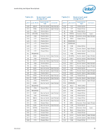
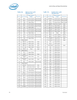
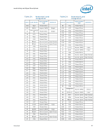
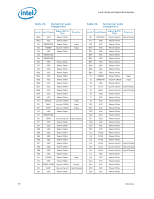
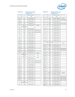
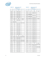
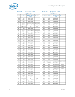
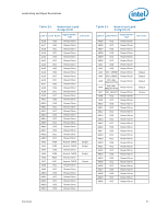
Land Listing and Signal Descriptions Table 24. Numerical Land Assignment Land # Land Name Signal Buffer Type Direction AB24 AB25 AB26 AB27 AB28 AB29 AB30 AC1 AC2 AC3 AC4 AC5 AC6 AC7 AC8 AC23 AC24 AC25 AC26 AC27 AC28 AC29 AC30 AD1 AD2 AD3 AD4 AD5 AD6 AD7 AD8 AD23 AD24 AD25 AD26 AD27 AD28 AD29 AD30 VSS VSS VSS VSS VSS VSS VSS TMS DBR# VSS RESERVED A25# VSS VSS VCC VCC VCC VCC VCC VCC VCC VCC VCC TDI BPM2# FC36 VSS ADSTB1# A22# VSS VCC VCC VCC VCC VCC VCC VCC VCC VCC Power/Other Power/Other Power/Other Power/Other Power/Other Power/Other Power/Other TAP Power/Other Power/Other Input Output Source Synch Input/Output Power/Other Power/Other Power/Other Power/Other Power/Other Power/Other Power/Other Power/Other Power/Other Power/Other Power/Other TAP Input Common Clock Input/Output Power/Other Power/Other Source Synch Input/Output Source Synch Input/Output Power/Other Power/Other Power/Other Power/Other Power/Other Power/Other Power/Other Power/Other Power/Other Power/Other Table 24. Numerical Land Assignment Land # Land Name Signal Buffer Type Direction AE1 AE2 AE3 AE4 AE5 AE6 AE7 AE8 AE9 AE10 AE11 AE12 AE13 AE14 AE15 AE16 AE17 AE18 AE19 AE20 AE21 AE22 AE23 AE24 AE25 AE26 AE27 AE28 AE29 AE30 AF1 AF2 AF3 AF4 AF5 AF6 AF7 AF8 AF9 TCK TAP Input VSS Power/Other FC18 Power/Other RESERVED VSS Power/Other RESERVED VSS Power/Other SKTOCC# Power/Other Output VCC Power/Other VSS Power/Other VCC Power/Other VCC Power/Other VSS Power/Other VCC Power/Other VCC Power/Other VSS Power/Other VSS Power/Other VCC Power/Other VCC Power/Other VSS Power/Other VCC Power/Other VCC Power/Other VCC Power/Other VSS Power/Other VSS Power/Other VSS Power/Other VSS Power/Other VSS Power/Other VSS Power/Other VSS Power/Other TDO TAP Output BPM4# Common Clock Input/Output VSS Power/Other A28# Source Synch Input/Output A27# Source Synch Input/Output VSS Power/Other VSS Power/Other VCC Power/Other VCC Power/Other 60 Datasheet
-
 1
1 -
2
-
3
-
4
-
5
-
6
-
7
-
8
-
9
-
10
-
11
-
12
-
13
-
14
-
15
-
16
-
17
-
18
-
19
-
20
-
21
-
22
-
23
-
24
-
25
-
26
-
27
-
28
-
29
-
30
-
31
-
32
-
33
-
34
-
35
-
36
-
37
-
38
-
39
-
40
-
41
-
42
-
43
-
44
-
45
-
46
-
47
-
48
-
49
-
50
-
51
-
52
-
53
-
54
-
 55
55 -
 56
56 -
 57
57 -
 58
58 -
 59
59 -
 60
60 -
 61
61 -
 62
62 -
 63
63 -
 64
64 -
 65
65 -
66
-
67
-
68
-
69
-
70
-
71
-
72
-
73
-
74
-
75
-
76
-
77
-
78
-
79
-
80
-
81
-
82
-
83
-
84
-
85
-
86
-
87
-
88
-
89
-
90
-
91
-
92
-
93
-
94
-
95
-
96
-
97
-
98
-
99
-
100
 |
 |