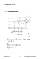
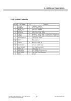
LG KM710 Service Manual - Page 39
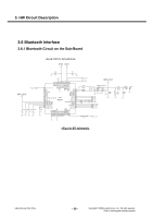
Bluetooth circuit Description
 |
View all LG KM710 manuals
Add to My Manuals
Save this manual to your list of manuals |
Page 39 highlights
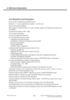
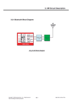
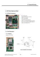
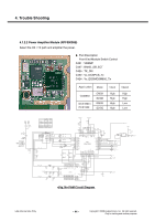
3. HW Circuit Description 3.6.3 Bluetooth circuit Description • Single chip 90 nm CMOS Bluetooth ROM solution • Bluetooth 1.1, 1.2 and 2.0 specification compliant - up to HCI level. • Enhanced Data Rate (2&3 Mbps) • Future support for Bluetooth 2005 core release (software upgrade when Bluetooth specification will be available) • Enhanced host interfaces (UART, SDIO) • Very low power consumption • Pin-to-pin compatible with BRF6150 • On-chip Digital Radio Processor (DRP) o Integrated 2.4 GHz RF transceiver o All digital PLL transmitter with digitally controlled oscillator o Near zero IF architecture o On-chip TX/RX switch o Support for Class 1 applications • Embedded ARM7TDMIE Microprocessor System On Chip o High rate H4 UART HCI o High rate HCI Three Wire UART Transport Layer (H5) o SDIO transport layer o Flexible PCM and I2S interfaces: full flexibility for data order, sampling and positioning o Automatic clock detection mechanism o Patch trap mechanism that enables feature changes in ROM (ROM updates, improvements) • On-chip Power Management adapted to cellular application o Direct connection to battery or external LDO 1.7 to 5.4V o IO supply voltage - 1.62 - 1.89V o Power saving mode o Shut-Down mode to minimize power consumption when Bluetooth is not used • Temperature detection and compensation mechanism ensures minimal variation in the RF performance over the whole temperature range • Seamless integration with TI OMAP™ application processor and GSM-GPRSUMTS chipset • Enhanced support for WLAN Co-existence (bandwidth sharing, antenna sharing) • Spurious emissions compatible with GPS applications • 5 external capacitors and balun/matching network required - total PCB area required only 45 mm2 (BGA package) • Package: 4.5x4.5 mm size, 0.5 mm ball pitch, pb-free Micro Star Junior BGA package. • Stacked RAM support with the same footprint as the ROM device (for development phase only) • TI proprietary low power scan achieves paging and inquiry scans with fast RSSI algorithm, at 1/3rd normal power. LGE Internal Use Only - 40 - Copyright © 2008 LG Electronics. Inc. All right reserved. Only for training and service purposes
-
 1
1 -
2
-
3
-
4
-
5
-
6
-
7
-
8
-
9
-
10
-
11
-
12
-
13
-
14
-
15
-
16
-
17
-
18
-
19
-
20
-
21
-
22
-
23
-
24
-
25
-
26
-
27
-
28
-
29
-
30
-
31
-
32
-
33
-
 34
34 -
 35
35 -
 36
36 -
 37
37 -
 38
38 -
 39
39 -
 40
40 -
 41
41 -
 42
42 -
 43
43 -
 44
44 -
45
-
46
-
47
-
48
-
49
-
50
-
51
-
52
-
53
-
54
-
55
-
56
-
57
-
58
-
59
-
60
-
61
-
62
-
63
-
64
-
65
-
66
-
67
-
68
-
69
-
70
-
71
-
72
-
73
-
74
-
75
-
76
-
77
-
78
-
79
-
80
-
81
-
82
-
83
-
84
-
85
-
86
-
87
-
88
-
89
-
90
-
91
-
92
-
93
-
94
-
95
-
96
-
97
-
98
-
99
-
100
-
101
-
102
-
103
-
104
-
105
-
106
-
107
-
108
-
109
-
110
-
111
-
112
-
113
-
114
-
115
-
116
-
117
-
118
-
119
-
120
-
121
-
122
-
123
-
124
-
125
-
126
-
127
-
128
-
129
-
130
-
131
-
132
-
133
-
134
-
135
-
136
-
137
-
138
-
139
-
140
-
141
-
142
-
143
-
144
-
145
-
146
-
147
-
148
-
149
-
150
-
151
-
152
-
153
-
154
-
155
-
156
-
157
-
158
-
159
-
160
-
161
-
162
-
163
-
164
-
165
-
166
-
167
-
168
-
169
-
170
-
171
-
172
-
173
-
174
 |
 |
