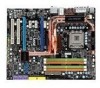
MSI MS-7512-010 User Guide - Page 64
BIOS Setup, Configuration DRAM Timing by SPD, MEMORY-Z, DIMM1/2/3/4 Memory SPD Information, DIMM 1/2
 |
UPC - 816909045635
View all MSI MS-7512-010 manuals
Add to My Manuals
Save this manual to your list of manuals |
Page 64 highlights
BIOS Setup tWR W hen the Configuration DRAM Timing by SPD is set to [Manual], the field is adjustable. It specifies the amount of delay (in clock cycles) that must elapse after the completion of a valid write operation, before an active bank can be precharged. This delay is required to guarantee that data in the write buffers can be written to the memory cells before precharge occurs. tWTR W hen the Configuration DRAM Timing by SPD is set to [Manual], the field is adjustable. This item controls the W rite Data In to Read Command Delay memory timing. This constitutes the minimum number of clock cycles that must occur between the last valid write operation and the next read command to the same internal bank of the DDR device. tRRD W hen the Configuration DRAM Timing by SPD sets to [Manual], the field is adjustable. Specifies the active-to-active delay of different banks. tRTP W hen the Configuration DRAM Timing by SPD sets to [Manual], time interval between a read and a precharge command. MEMORY-Z Press to enter the sub-menu and the following screen appears. DIMM1/2/3/4 Memory SPD Information Press to enter the sub-menu and the following screen appears. DIM M 1/2/3/4 Memory SPD Information These items display the current status of the current DIMM Memory speed information such as momory type, max bandwidth, manufacture, part number, serial number, SDRAM cycle time, DRAM TCL, DRAM TRCD, DRAM TRP, DRAM TRAS, DRAM TRFC, DRAM TWR, DRAM TWTR, DRAM TRRD and DRAM TRTP. They are read only. 3-21
-
 1
1 -
2
-
3
-
4
-
5
-
6
-
7
-
8
-
9
-
10
-
11
-
12
-
13
-
14
-
15
-
16
-
17
-
18
-
19
-
20
-
21
-
22
-
23
-
24
-
25
-
26
-
27
-
28
-
29
-
30
-
31
-
32
-
33
-
34
-
35
-
36
-
37
-
38
-
39
-
40
-
41
-
42
-
43
-
44
-
45
-
46
-
47
-
48
-
49
-
50
-
51
-
52
-
53
-
54
-
55
-
56
-
57
-
58
-
 59
59 -
 60
60 -
 61
61 -
 62
62 -
 63
63 -
 64
64 -
 65
65 -
 66
66 -
 67
67 -
 68
68 -
 69
69 -
70
-
71
-
72
-
73
-
74
-
75
-
76
-
77
-
78
-
79
-
80
-
81
-
82
-
83
-
84
-
85
-
86
-
87
-
88
-
89
-
90
-
91
-
92
-
93
-
94
-
95
-
96
-
97
-
98
-
99
-
100
-
101
-
102
-
103
-
104
-
105
-
106
-
107
-
108
-
109
-
110
-
111
-
112
-
113
-
114
-
115
-
116
-
117
-
118
-
119
-
120
-
121
-
122
-
123
-
124
-
125
-
126
-
127
-
128
-
129
-
130
-
131
-
132
-
133
-
134
-
135
-
136
-
137
-
138
-
139
-
140
-
141
-
142
-
143
-
144
-
145
-
146
-
147
 |
 |
