Oki ML421 Maintenance Manual - Page 127
Circuit Description
 |
View all Oki ML421 manuals
Add to My Manuals
Save this manual to your list of manuals |
Page 127 highlights
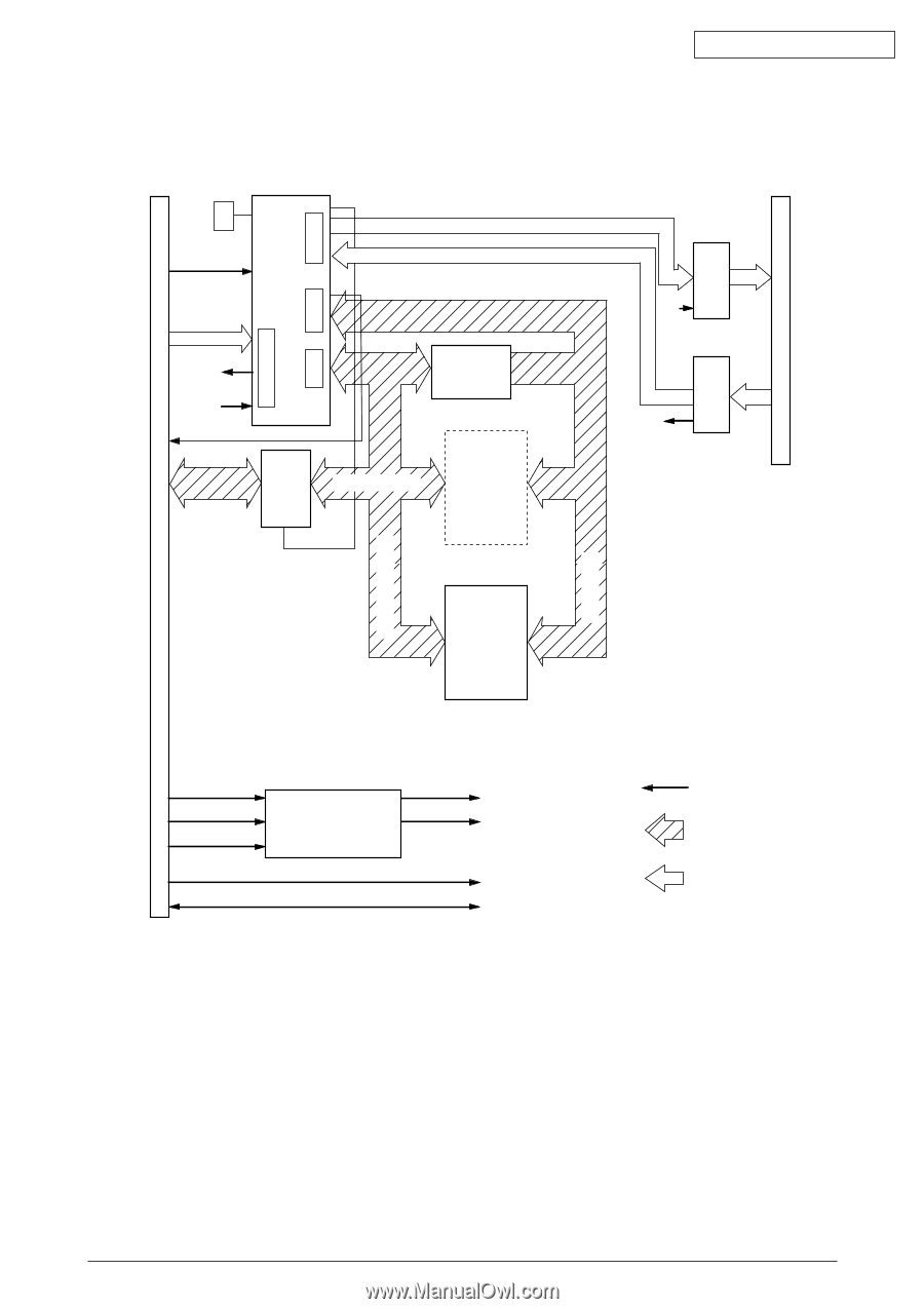
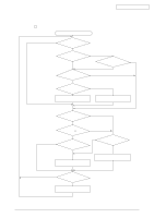
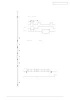
2.2 Circuit Description A block diagram is shown in Figure C-1. 80C51 RST OCS P1 P3 P0 P2 TD RD IF WR ADR latch LS245 DB0 to DB9 ROM 64Kbit Receiver Driver Oki Data CONFIDENTIAL CN1 75188 TD 75189 RD ADR bus ADR/data bus RAM 64Kbit +5 VD +12VDC -8VDC +5 V ±9 V power supply circuit +9 V -9 V +5V 0V Figure C-1 Block Diagram Serial data control line Bus line Control line 2.2.1 Operation at power on After power is turned on, an RST OUT signal is sent from the printer control board to reset the printer. When the reset is canceled, the 80C51 CPU performs initialization. Initialization consists of setting the 80C51 timer, and setting the serial mode. 2.2.2. RS-232C interface The DTR, SSD, TD and RTS signals output by the 80C51 are converted to RS-232C signals by line driver 75188 (Q1) and sent to the interface. In addition, signals DSR, CTS, CD, and RD on the RS232C interface are converted to TTL level by line receiver 75189 (Q2) and input to the 80C51. 42113901 Rev.2 127 /
-
 1
1 -
2
-
3
-
4
-
5
-
6
-
7
-
8
-
9
-
10
-
11
-
12
-
13
-
14
-
15
-
16
-
17
-
18
-
19
-
20
-
21
-
22
-
23
-
24
-
25
-
26
-
27
-
28
-
29
-
30
-
31
-
32
-
33
-
34
-
35
-
36
-
37
-
38
-
39
-
40
-
41
-
42
-
43
-
44
-
45
-
46
-
47
-
48
-
49
-
50
-
51
-
52
-
53
-
54
-
55
-
56
-
57
-
58
-
59
-
60
-
61
-
62
-
63
-
64
-
65
-
66
-
67
-
68
-
69
-
70
-
71
-
72
-
73
-
74
-
75
-
76
-
77
-
78
-
79
-
80
-
81
-
82
-
83
-
84
-
85
-
86
-
87
-
88
-
89
-
90
-
91
-
92
-
93
-
94
-
95
-
96
-
97
-
98
-
99
-
100
-
101
-
102
-
103
-
104
-
105
-
106
-
107
-
108
-
109
-
110
-
111
-
112
-
113
-
114
-
115
-
116
-
117
-
118
-
119
-
120
-
121
-
 122
122 -
 123
123 -
 124
124 -
 125
125 -
 126
126 -
 127
127 -
 128
128 -
 129
129 -
 130
130 -
 131
131 -
 132
132 -
133
 |
 |